Bedtime reading, right here, at DIYAudio!
http://www.diyaudio.com/forums/diya...udio-component-grounding-interconnection.html
http://www.diyaudio.com/forums/diya...udio-component-grounding-interconnection.html

I went back to post #753 and looked at both schematics. There isn't a 33k on them.I am planning to use Daniel's 33K recommendation, though.
edit: Just checked again. And still no 33k. That was just like: "Is the coffeepot on?" because I'd have to go check it every time.
I went back to post #753 and looked at both schematics. There isn't a 33k on them.
edit: Just checked again. And still no 33k. That was just like: "Is the coffeepot on?" because I'd have to go check it every time.
I claim dyslexia. Yes, that's right! 25k no substitution. I must have gotten 33 in my mind from the bootstrap capacitor? Good catch!. Some days I spend minutes looking for my keys, only to find they are still in the lock. Now I always check the lock when I can't find my keys.
Sixto 🙄
Passenger side car door, or if summertime, randomly in the freezer.I claim dyslexia. Yes, that's right! 25k no substitution. I must have gotten 33 in my mind from the bootstrap capacitor? Good catch!. Some days I spend minutes looking for my keys, only to find they are still in the lock. Now I always check the lock when I can't find my keys. Sixto 🙄
TAXI!!!
Input loadI claim dyslexia. Yes, that's right! 25k no substitution.
You can use a 25k trimmer for input load if you want to. It can vary the midrange tone.
Feedback resistor
In two days time, I did solder on every resistor value to test results.
That is fine within the narrow range of 25k to 27k.
An alternative with minimal costs is 47k (for use in case you need to set the input load up as high as 47k to support tube/valve sources).
This post applies to TDA7293-Mar V6 and TDA7294S-singapore...real TDA7294S cores that have all 15 pins working. Verify that and then proceed.
That question--Speaker ground = power ground.
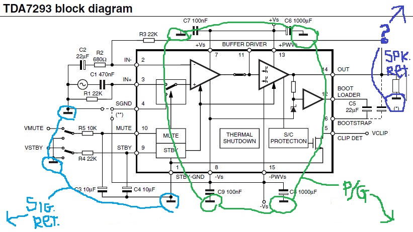
Your negative feedback is a circuit. And circuit means loop, which does require a return. The negative feedback makes a small to large signal transition. The return for that one is the 0v at the amplifier board.
If one can momentarily overlook the vexing pinout and succeed nevertheless (postage stamp sized board?), then Pins 1, 7, 8 on the schematic that you posted, all have the same 0v.
Standby circuit is located at the output of the small signal voltage amp and belongs to voltage amp power group.
Mute circuit is located at the Input of the small signal voltage amp and belongs to small signal input group.
It is not especially erroneous to assign pin1 return to small signal, because indeed the current is really very tiny, and because, assuring the absence of layout foobar despite vexing pinout makes the board so small that the whole business is buss ground and a moot point. The discussion of separated grounds is only relevant to a large sprawling layout that would inherently assure instability. No dice. Don't even worry about it, but instead, just buy a tiny board and then route the signal resistors directly, by shortest path, under-board, instead of the popular combination of decorative and dysfunctional placement.
Basically, the available boards don't support the ideals.
That reminds me that I really have some layout work labors to do before producing a kit for these things; but, at long last, it has begun to look possible.
Last edited:
Here is a careful start to a layout. I like the way pins 13-14-15 and 7-8 are grouped together, should make the supply and ground routing easier.
Thanks Mark, you don't think it would be a noise potential to connect all the grounds on each amp board? I 've been reading multiple recommendations to keep the signal returns separate from the psu ground, but join them with wires off the board, in a star-ground configuration. Then add the chassis ground, though isolated from the other two with a C and R in parallel.
I've been also wondering if a small diode where the signal ground connects to the power ground might help prevent PSU noise from flowing on to the signal circuits?
Still sleepy, (but sometimes that's where the best ideas come from)
Sixto.
The discussion of separated grounds is only relevant to a large sprawling layout that would inherently assure instability...Basically, the available boards don't support the ideals.
Aha! - that explains it. Ok, I can understand this... none of the publications I've read talk about board size. They are just dealing with abstract ideal concepts. Thanks for bringing it down to my level of understanding.
(I was having coffee, and pondering my previous post when you posted your response)
Sixto.
I put in an extra resistor (1R or less) between input ground and power ground, If you do this on every channel then add a ground loop breaker between the power ground and the chassis/PE, you should have no problem with ground loop noise.
I put in an extra resistor (1R or less) between input ground and power ground, If you do this on every channel then add a ground loop breaker between the power ground and the chassis/PE, you should have no problem with ground loop noise.
Ok, this sounds simple and easy enough to do, it's that whole question about insurance, I really hate paying for it, until I need it.
Thanks Mark!
Sixto.
Indeed we continue to be in need of a goal to shoot for. AndrewT has illustrated what that could be, and we are grateful.Aha! - that explains it. Ok, I can understand this... none of the publications I've read talk about board size. They are just dealing with abstract ideal concepts.
When we, finally, manage to do the technical ideals without a terrible compromise to practicality, then it has been a very fine art.
I have been getting closer, but that hasn't been going quickly, and there is a lot more to do.
I refuse to give up on practical performance because it is necessary, but then how do you accommodate technical idealism? Push forth because it is rewarding.
So I'd have to disagree that the concepts are abstract. They're not abstract--they are relevant.
In fact, they're really very inconvenient and we can't progress further without them.
That will not be fast.
Nope! I would much prefer to believe that I had managed to bring it UP to your level of understanding.Thanks for bringing it down to my level of understanding.
Last edited:
Not so sure if it does anything for audio, either for or against. But, I'm very sure that it will promote good layout and understanding as well. Let's consider it mandatory, because we are, for sure, in need of good layout. Your concept forces good layout. Yeah, that's alright.I put in an extra resistor (1R or less) between input ground and power ground, If you do this on every channel then add a ground loop breaker between the power ground and the chassis/PE, you should have no problem with ground loop noise.
The great part about this design is that the 1R resistor is optional, replace it with a wire and you still have the best ground layout. If I can find the time I will make a start on a PCB design.
The decoupling and boostrap caps all go as close as possible to the chip.The great part about this design is that the 1R resistor is optional, replace it with a wire and you still have the best ground layout. If I can find the time I will make a start on a PCB design.
Where the majority of designs have failed is being overtly concerned about the standby and mute features; and, therefore I suggest to tack them on lastly.
The bootstrap cap can be 33u or 47u.I must have gotten 33 in my mind from the bootstrap capacitor?
Generally, 47u could be good for a woofer or subwoofer amplifier.
The same datasheet that lists a too small value in the schematic also mentions to increase it, had you wanted goodly bass. The text portion of the datasheet is quite useful!
If I can find the time I will make a start on a PCB design.
Don't know if I can be much help there, but I'm definitely interested, and would love to contribute some thoughts... One thing I've read in other posts is that people often lament having to place the TDA7293 chip so close to one edge of the board (due to heatsink requirements). I wonder why we couldn't place all the bulky components on the bottom, and keep only short components such as resistors and connector terminals on top. This would allow placing the chip more to the center of the board, with closer placement of surrounding elements to their pins (and ground/power traces) on all 4 sides, and still leave enough room for a heatsink to float above all that, and even span 2 or 3 boards!
Another idea I first saw on Daniel's P2P thread is how easy it is to solder the feedback resistor and bootstrap capacitors right on the pins. Don't have to do a lot more than that to save some board space that can be used for other components. And who says everything has to be on the board?
Third, is one of the boards I got as sample, had a number of vias touching the chip-pin vias. Almost like a P2P layout (or next closest thing!).
Who knows, maybe my 30 years of bricks-and-mortar architecture and design background can contribute something? I can almost visualize this thing in 3-d space. (too bad I don't know how to use PCB layout software...yet)
Sixto.

This is so... (wait for it)
COOL !!!
COOL !!!
Work in progress. Datasheet figure 1
Stability (and potentially resolution/imaging/realism) is improved by locating C6 and C8 decoupling caps Much Closer to pins 7 and 8.
In my opinion the compromise of having accessories like R6, C7, C9 push the decoupling caps farther away from the chip, couldn't possibly be worth what that costs.
P.S.
The feedback-shunt, R1 and associated coupling cap(s), C2 are positioned nicely! Love the orientation of C2, in case I need to add more caps off the edge of the board, it is super easy. THANKS!!!! Might suggest making R1 vias both resistor and cermet trimmer compatible--that dial can buy 2x lower gain.
Last edited:
- Home
- Amplifiers
- Chip Amps
- Optimizing TDA7294 Output