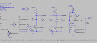
Hi, i am working on a power amplifier with ON-Semi Thermaltrak Transistors.
As the NPN and PNP devices are positioned at the opposite sides of my board
layout, the traces between the thermaltrak diodes get quite long. I worry that
these track which are signal lines from the VAS could be quite sensitive to
external noise.
So, my idea was to isolate the thermaltrak diodes optically from the bias
spreader so that the traces with the VAS signal get shorter and less sensitive.
I have to say that i am not a specialist on that topic. I have read a lot in this
forum from Bob Cordell, D. Self and others. But i am not really able to judge if
my idea will work the way i designed it.
I can at least say that tempco will not be compensated sufficiently at the moment.
I will return to that topic when the optoisolation works.
What do you think? Will that work?
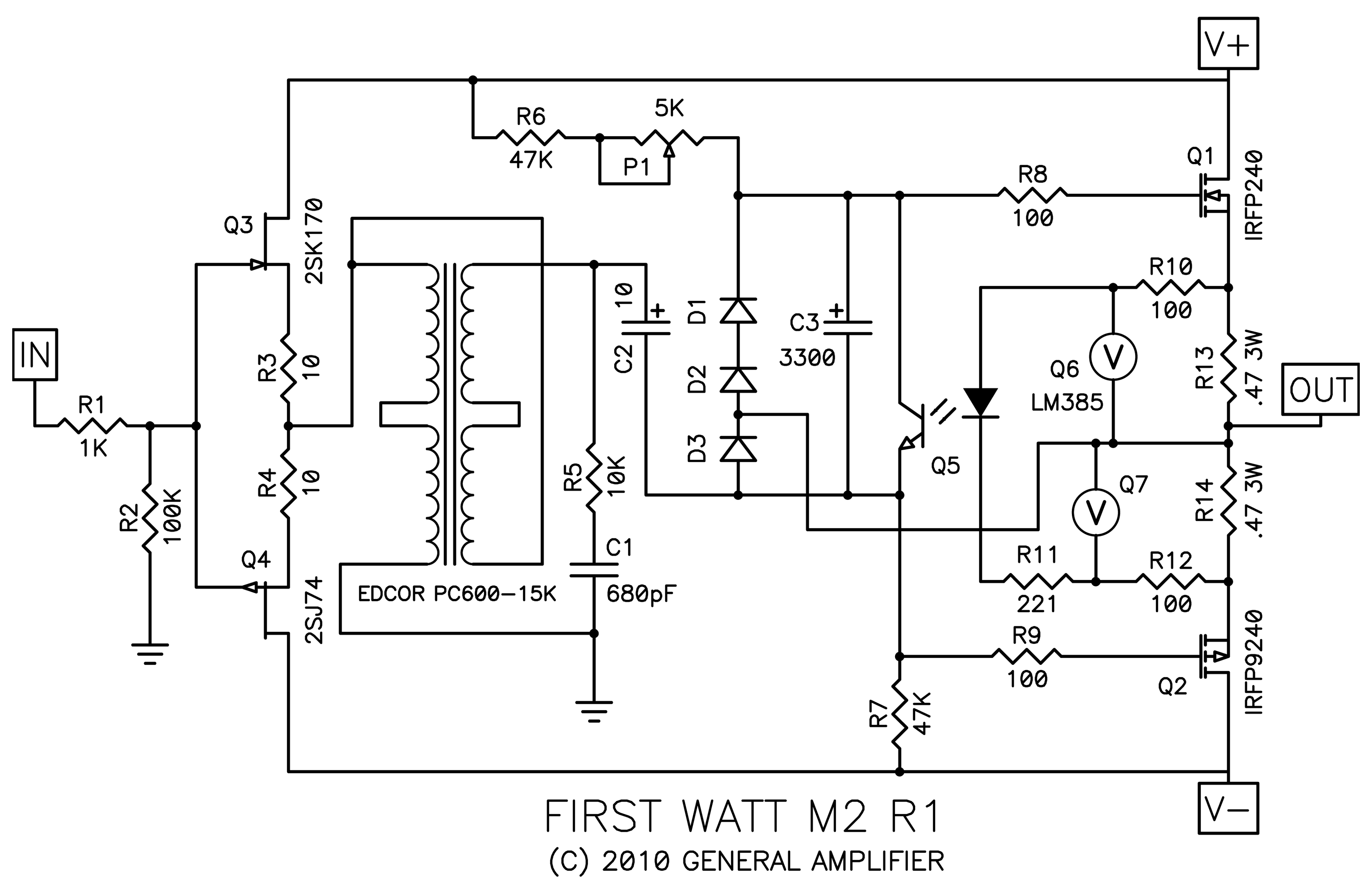
See my schematic below:
As the NPN and PNP devices are positioned at the opposite sides of my board
layout, the traces between the thermaltrak diodes get quite long. I worry that
these track which are signal lines from the VAS could be quite sensitive to
external noise.
So, my idea was to isolate the thermaltrak diodes optically from the bias
spreader so that the traces with the VAS signal get shorter and less sensitive.
I have to say that i am not a specialist on that topic. I have read a lot in this
forum from Bob Cordell, D. Self and others. But i am not really able to judge if
my idea will work the way i designed it.
I can at least say that tempco will not be compensated sufficiently at the moment.
I will return to that topic when the optoisolation works.
What do you think? Will that work?
See my schematic below:
Attachments
Hi Elfenthau,
On one hand - interesting project. In fact, you need to design an optically coupled "bias repeater".
On the other hand - I don't really see too much of practical advantage. Using SMD parts, it's possible to arrange the layout in such a way, that VAS output will be close enough to the output devices. Moreover, VAS output is normally pretty powerful (5-7mA of quiescent current) for being "insensitive" enough.
Cheers,
Valery
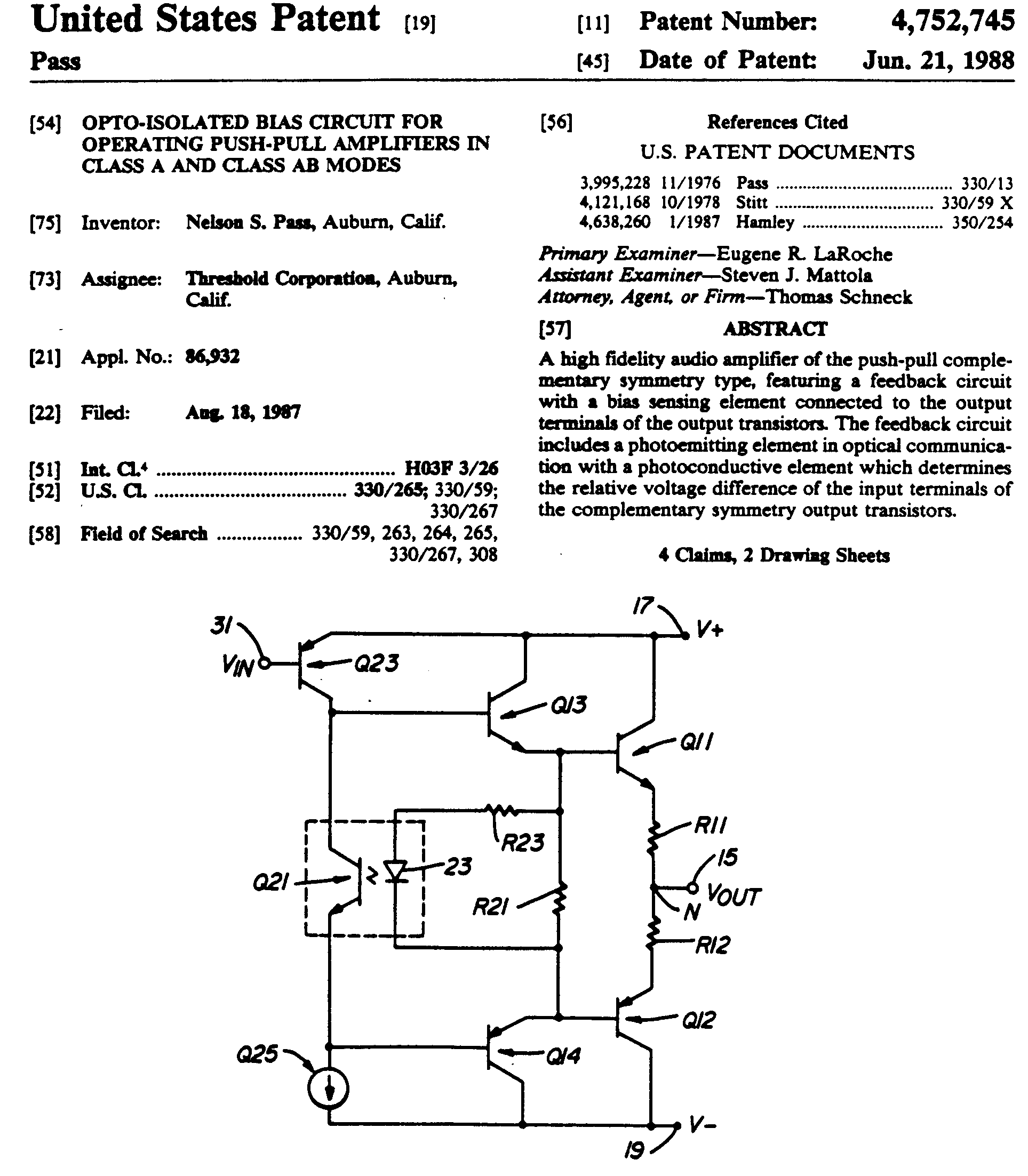
Here is a source for inspiration:optocoupler where the optocoupler transistor replaces the spreader transistor usually used? May be i should try that.
http://www.diyaudio.com/forums/solid-state/251135-opto-controlled-bias.html
Very interesting. So i could make the things even simpler using a standart transistor
optocoupler where the optocoupler transistor replaces the spreader transistor usually used? May be i should try that.
Thanks xrk971!
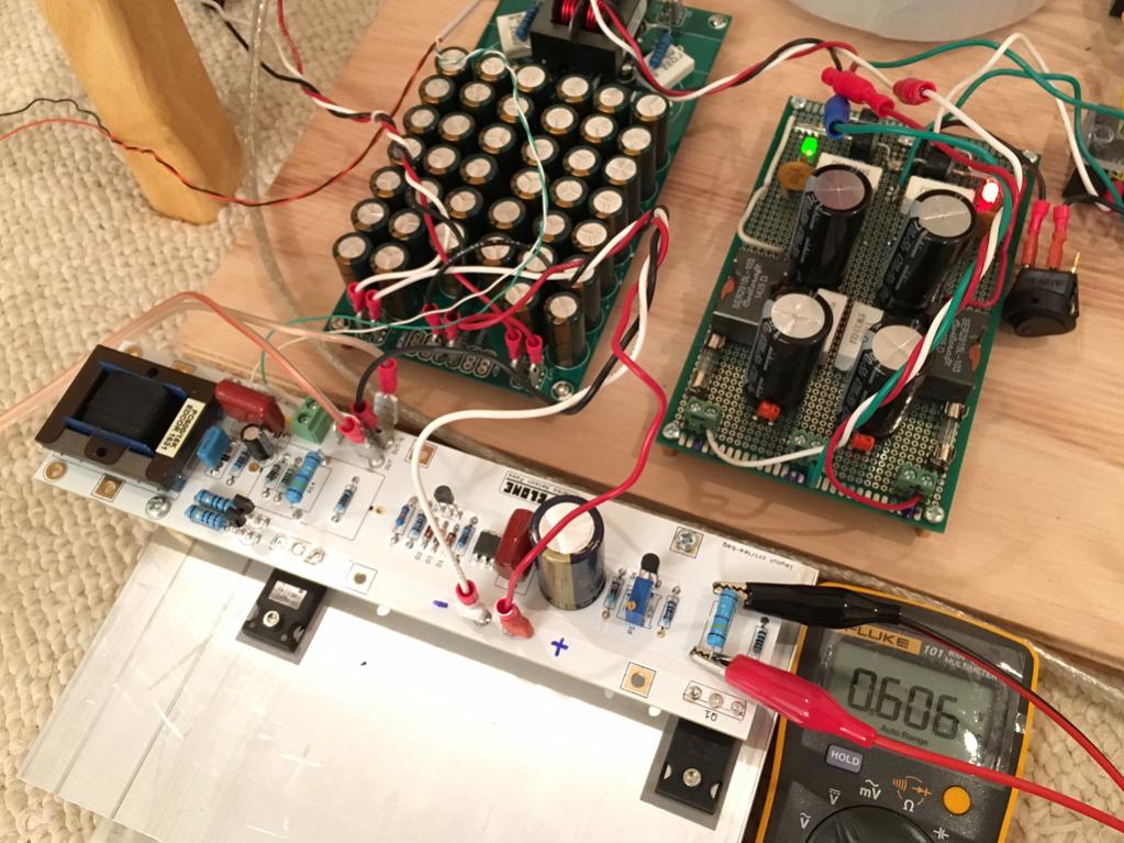
This setup on M2 works superbly for controlling bias on class A operation with hexFETs and no temperature feedback needed as it senses the current applied directly. Very stable. I want to apply this to my other amps. The opto coupler is not expensive and the two 1.2v precision voltage reference IC's (LM385LP-1-2) are not either.
Here it is on my M2 showing rock stable 0.606v across 0.47R power resistor. The way Pass designed this circuit - it has a slow time constant but that works well for matching time constant of heatsink.
Last edited:
Leach Vbe circuit: With the diodes on the heatsink, resistors on the circuit board can be used in series with the diode-wires to isolate this capacitance from the second stage.
Naturally, a different physical construction where the input+VAS+Vbe are on the same PCB, and close to the temperature sense diodes/transistor PCB traces is a good goal.
Naturally, a different physical construction where the input+VAS+Vbe are on the same PCB, and close to the temperature sense diodes/transistor PCB traces is a good goal.
Attachments
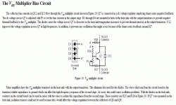
Those 4 diodes could be the Thermal Track diodes in a 2pair output stage.
They can be used in a Leach style Vbe multiplier.
Or they can be used directly to set the bias voltage required to hold the output stage bases at the required voltage difference to remain in optimal ClassAB bias.
In either of the above topologies you would need to set the tempco of the diodes to suit the output stage requirement.
That is usually done by adjusting the diode current.
The -2.2mV/C often seen stated for silicon diodes only holds at one current density. Change the current density through the junction and you get a different tempco. I have seen variations from -1.8mV/C to -2.3mv/C dependant on the current.
 , but they were a bit pricey.
- Status
- This old topic is closed. If you want to reopen this topic, contact a moderator using the "Report Post" button.
- Home
- Amplifiers
- Solid State
- Optically isolated thermaltrak bias spreader