Hi all,
I've been in audio hiatus for a couple of years, but recently upgraded my PS3+Dacmagic combo to the fanless (yay!) Oppo BDP105D. Out of the box it sounds better than the modded Dacmagic (even when the Dacmagic is fed through coax).
A short double-blind comparison with a Krell SBP-32X (a Krell with improved output coupling caps, with the Oppo as coax SPDIF source for the Krell, both connected to the pre-amp via RCA) reveals that the Krell is able to produce more detail from 44.1kHz/16b material (really, you hear things that the stock Oppo masks), so I'm looking to do some soldering to improve the Oppo.
The fact that the Krell can create more detail from the same digital data stream leads me to believe that the main limitation lies in any of the following:
I've selectively looked through this thread, and while I can see a schematic of the analog stereo output board (which is the one I intend to modify), I didn't find anything related to the supply design. Maybe someone can PM me a service manual?
Two other questions I have:
1. Are the resistors in the I/V feedback really different, as indicated in the schematic? I haven't opened up the Oppo yet, so I hope someone who did open it up can shed some light on this.
2. Is it common to have an emitter-follower Op-Amp such as the LM(E)4562 used as I/V converter following the ESS Sabre DAC? Would it be a bad idea to substitute a rail-rail output stage Op-Amp and do the class-A biasing to the V+ rail?
Cheers!
I've been in audio hiatus for a couple of years, but recently upgraded my PS3+Dacmagic combo to the fanless (yay!) Oppo BDP105D. Out of the box it sounds better than the modded Dacmagic (even when the Dacmagic is fed through coax).
A short double-blind comparison with a Krell SBP-32X (a Krell with improved output coupling caps, with the Oppo as coax SPDIF source for the Krell, both connected to the pre-amp via RCA) reveals that the Krell is able to produce more detail from 44.1kHz/16b material (really, you hear things that the stock Oppo masks), so I'm looking to do some soldering to improve the Oppo.
The fact that the Krell can create more detail from the same digital data stream leads me to believe that the main limitation lies in any of the following:
- Limited supply regulation on the ESS DAC IC
- Limited supply regulation on any of the LM(E)4562s following the DAC IC
- Distortion from the electrolytic output coupling caps
- Distortion from the 100 pF feedback caps in the I/V amplification stage
- Distortion from the 330 pF feedback caps in the buffer amplification stage
I've selectively looked through this thread, and while I can see a schematic of the analog stereo output board (which is the one I intend to modify), I didn't find anything related to the supply design. Maybe someone can PM me a service manual?
Two other questions I have:
1. Are the resistors in the I/V feedback really different, as indicated in the schematic? I haven't opened up the Oppo yet, so I hope someone who did open it up can shed some light on this.
2. Is it common to have an emitter-follower Op-Amp such as the LM(E)4562 used as I/V converter following the ESS Sabre DAC? Would it be a bad idea to substitute a rail-rail output stage Op-Amp and do the class-A biasing to the V+ rail?
Cheers!
Joe,
How does the Oppo provide the offset value to the differential opamps. Is that from the 9018 or a separate circuit that supplies the value. Also, it would seem likely the different gains in the I/V converter would cause output offset voltage, looking at the ESS data both values are the same. Having said that I'm sure there is some reason that Oppo did this, is this something you can explain.
Thanks
James
Some interesting clarifications from Oppo (published in AVForum):
Q1. What op-amps are you using in the 105? Are they the same amps used in the 95?
A1. For the BDP-105 we are using the same op-amps as the BDP-95, the LME4562.
Q2. Would you please let me know how the output ESS9018 DAC is configured for the analog stereo outputs and headphone amplifier? For the 83SE and the 95, 4 dacs were dedicated to each stereo and XLR channel for a 4+4 configuration. Is it 2+2 for the XLR channels, 1+1 for the RCA and 1+1 for the headphone amplifier channels? The concern is that the 105 will have inferior analog specs(SNR, THD etc) when compared to the excellent BDP-95.
A2. We want to ensure you that the BDP-105 has the same analog specifications and performance as the BDP-95. This has been a requirement for our design and engineering team from the very beginning of the BDP-105 project. It is also the reason for the new DAC configuration.
In the BDP-105's stereo board design, the 4 pairs of DACs in the ES9018 DAC are allocated as: 1 pair for the RCA outputs, 1 pair for the XLR outputs, and 2 pairs stacked for the headphone amplifier. We had incorrectly stated in the past that 1 DAC pair was used as a ground. This was at one time true as we were working on the engineering, but the final production model which will be shipping to customers will not use a 1 DAC pair for the ground.
During the initial design stage, we simply continued the BDP-95 approach by stacking 4 pairs of DAC for each L/R channel. However due to the complexity brought in by the newly added headphone amp and USB DAC, we could not achieve an ideal PCB layout. The analog specifications became slightly worse than the BDP-95 in this 4 stacked configuration. Our audio engineers and consultants analyzed the problem and made many experiments to further enhance the quality of the analog output stage of the BDP-105. In the end, they decided that the only way to ensure maximum performance was to separate the current-to-voltage conversion stages for each output path. This change enables us to have a much cleaner PCB layout which minimizes interference and crosstalk. It also eliminates the possibility of the load on one output path affecting the other paths. The drawback is that we now lose the benefit of the thermal noise cancellation by stacking 4 DACs. The engineers were able to make up for that by designing an improved power supply, optimizing the filter and drive stages, and beefing up the power and ground paths. The new design costs more than the BDP-95's stereo outputs so it is absolutely not a cost cutting measure. We end up using more high performance components such as op-amps, WIMA and ELNA capacitors.
We try to give conservative, nominal specifications in any literature that we produce, even when the player is known to exceed them. We list the BDP-95's THD+N as -110dB. In our own test it was -114dB. The BDP-105's THD+N is also listed as -110dB. In our own test it was between -115 or -116dB, slightly better than the BDP-95.
The headphone amplifier gets 2 pairs of DAC because its load is much higher than line-level RCA and XLR outputs.
Q3. Are the BDP-105 analog outputs AC or DC coupled? The 95 and 83SE outputs were DC coupled. If the 105 outputs are AC coupled, can you tell us why this is the case?
A3. The BDP-105 analog outputs are AC coupled. The BDP-95 used DC coupled output, and we have had a few rare but annoying compatibility issues with certain amplifiers. Some amplifier may have a DC offset on its input and that has caused issues from popping noises, degraded sound to damaged players. We have selected the components carefully so that the AC coupled output can still produce excellent bass response. The capacitors used are high quality ELNA capacitors. Again this increases cost so we do not make this kind of design changes without a good reason. For the unbalanced RCA stereo output, our consultant developed a certain way to bias the components so it actually sounds and measures better than the BDP-95, but requires an AC coupled output.
Overall we believe that the BDP-105 sounds slightly better than the BDP-95 due to these design changes. In the end, one has to listen to the player to draw a conclusion. When we first got the ES9018 reference design board a more than two years ago, it measured extremely well but sounded completely "dead". We almost decided against using it and went back to the ES9016 until we actually built our own board to test and found that the ES9018 was indeed better. Audio engineering is a combination of craft and science, and sometimes what is good in theory does not translate to good sound. Our design decisions were based on many years of collective experience from our engineers and consultants, as well as test results from many revisions, and never on cost reduction.
Q4. Would it be possible via a FW update for the user to select in the user menu the maximum power output for the headphone amplifier? The reason i'm asking is that some rather exotic headphones have low sensitivity (electro-statics for example) and need hundreds of milli-watts to come alive, some even requiring a watt or more. A few popular examples would be:
1. Hifiman HE-6 with 83dB/mW @50-ohms impedance.
2. AKG K1000 with 74dB/mW @120-ohms impedance.
A4. Unfortunately it is not possible to adjust the player's maximum power through the headphone amplifier through the firmware. We had toyed with this implementation, but we have found that this could cause loss of resolution and detail when handled through software.
The ability to adjust the maximum power will have to be done through physical hardware (capacitor replacement).
We have tried a wide range of headphones on our players, and based on subjective listening, we have not found a headphone which we felt was not being driven comfortably at the highest volume level when using the headphone amplifier.
It may very well be possible that there are headphones which are incredibly hard to drive, and once encountered, there may be the possibility of swapping out the headphone amplifier which has been modified to better suit the headphone. We will stress that this is a huge "may" as we have never been a fan of after market solutions, but we have done them in the past with the BDP-83 RS232 and BDP-83SE upgrade kits.
interesting insights. Can you elaborate on deciding on The polatity of The Elna electrolytic as opamp offset polarity is unpredictable. Or do you force The output offset voltaje in a given direction?
Well, is quite a time ago this post was written... I almost forgot I written it (or copy/paste it)...
Yes, indeed, the polarity of the output stage offset it unpredictable, and this is because the impossibility of producing two perfectly identical (opamps) circuits, with perfect match parameters, even when these are on the same die.
In my opinion, there is wrong to use polarised caps in this place. What it is the clue with such caps in this place, and not the right ones? The right rule here is to be used unipolar caps. I do not know why the designers chosen so, as the unipolar caps are not specially expensive comparing with these Elna ones... Whatever...
In the beginning of this thread I supported the idea of a DC coupled output, and removing of these caps. Well, one can chose so, if one can set it up the opamps for a slightly zero offset. However, I found out that it may be quite difficult to fix a zero offset, and quite unsafe in some cases to have a DC coupling on outputs. As it is very difficult to reach a 0,000v offset in a repetitive way, I decided to adopt the Oppo`s idea with AC coupling for my mod - output module, but doing it right. I mean using the unipolar caps. With the right AC coupling caps configuration, one get the completely audio signal transparency for this AC coupling approach. So, it is also established a quite wide compatibility with the power amps out here. I go on the AC coupling way, as my output module is based on OPA1632, which it however have few mV unpredictable offset, and is more safe for compatibility. Doing it the AC coupling with the right components, and in the right way, it leads to very good results.
As a rule, in particular cases, one should measure the DC offset on the outputs (before these caps) for his own device, before eventually remove these caps (to get DC coupling), if one may conclude it may be safe so for the own power amp.
However the original caps should be replaced or bypassed.
Because this subject here (AC coupling - offset) it may be tied to the previous posts too, I chose the opportunity to answer to jewilson, even though I`m not Joe, as partially an answer for MatchASM questions.
The resistors in the I/V feedback are indeed different as values. There is a explanation for this design in post 1421 (ignore the bad words referring to me...). As i remember, Joe had too an explanation about this subject. Please search back into the thread.
Well, my opinion is to be used here the ESS recommended symmetrical design (ESS9018 datasheet). This makes much more sense to me.
The offset control on Oppo players I/V design is provided by a quite simple circuit deriving from AVCC regulator. The AVCC regulated tension it is divided to some 1,xxxV ( I do not remember well about this value), and it goes through a a long trace all over the stereo board, to each involved opamp offset pins. A test point for this offset tension control is to be found on stereo board.
In my opinion, this design is just wrong. No matter how well it is filtered and regulated the AVCC (by the way a wrong regulator design here too), there is a residual ripple on this rail, as some other noises (collected by a long trace), which are induced into the offset pin of the opamps. Why so, and not just putting it this pin to the ground? What advantages it can bring such design for the audio signal quality? Why complicated instead of simple design? Well, ask Oppo designers...
Yes, indeed, the polarity of the output stage offset it unpredictable, and this is because the impossibility of producing two perfectly identical (opamps) circuits, with perfect match parameters, even when these are on the same die.
In my opinion, there is wrong to use polarised caps in this place. What it is the clue with such caps in this place, and not the right ones? The right rule here is to be used unipolar caps. I do not know why the designers chosen so, as the unipolar caps are not specially expensive comparing with these Elna ones... Whatever...
In the beginning of this thread I supported the idea of a DC coupled output, and removing of these caps. Well, one can chose so, if one can set it up the opamps for a slightly zero offset. However, I found out that it may be quite difficult to fix a zero offset, and quite unsafe in some cases to have a DC coupling on outputs. As it is very difficult to reach a 0,000v offset in a repetitive way, I decided to adopt the Oppo`s idea with AC coupling for my mod - output module, but doing it right. I mean using the unipolar caps. With the right AC coupling caps configuration, one get the completely audio signal transparency for this AC coupling approach. So, it is also established a quite wide compatibility with the power amps out here. I go on the AC coupling way, as my output module is based on OPA1632, which it however have few mV unpredictable offset, and is more safe for compatibility. Doing it the AC coupling with the right components, and in the right way, it leads to very good results.
As a rule, in particular cases, one should measure the DC offset on the outputs (before these caps) for his own device, before eventually remove these caps (to get DC coupling), if one may conclude it may be safe so for the own power amp.
However the original caps should be replaced or bypassed.
Because this subject here (AC coupling - offset) it may be tied to the previous posts too, I chose the opportunity to answer to jewilson, even though I`m not Joe, as partially an answer for MatchASM questions.
The resistors in the I/V feedback are indeed different as values. There is a explanation for this design in post 1421 (ignore the bad words referring to me...
). As i remember, Joe had too an explanation about this subject. Please search back into the thread.Well, my opinion is to be used here the ESS recommended symmetrical design (ESS9018 datasheet). This makes much more sense to me.
The offset control on Oppo players I/V design is provided by a quite simple circuit deriving from AVCC regulator. The AVCC regulated tension it is divided to some 1,xxxV ( I do not remember well about this value), and it goes through a a long trace all over the stereo board, to each involved opamp offset pins. A test point for this offset tension control is to be found on stereo board.
In my opinion, this design is just wrong. No matter how well it is filtered and regulated the AVCC (by the way a wrong regulator design here too), there is a residual ripple on this rail, as some other noises (collected by a long trace), which are induced into the offset pin of the opamps. Why so, and not just putting it this pin to the ground? What advantages it can bring such design for the audio signal quality? Why complicated instead of simple design? Well, ask Oppo designers...
Hi Coris,
Thanks for your reply.
All I have right now is a schematic of the analog stereo output board. The only thing that makes me happy about that schematic is seeing the arrangement of the relay for muting.
Thanks for your reply.
This seems like poor design. If really true, some of the output caps will depolarize over time. Wasn't there a statement from Oppo saying there was a systematic offset on the output? That would contradict the above.Yes, indeed, the polarity of the output stage offset it unpredictable, and this is because the impossibility of producing two perfectly identical (opamps) circuits, with perfect match parameters, even when these are on the same die.
Well, maybe the ESS design is especially better if the power supply is properly implemented.The resistors in the I/V feedback are indeed different as values. There is a explanation for this design in post 1421 (ignore the bad words referring to me...
Well, my opinion is to be used here the ESS recommended symmetrical design (ESS9018 datasheet). This makes much more sense to me.
I imagine this has to do with cost. Are schematics of the AVDD regulator available?The offset control on Oppo players I/V design is provided by a quite simple circuit deriving from AVCC regulator. The AVCC regulated tension it is divided to some 1,xxxV ( I do not remember well about this value), and it goes through a a long trace all over the stereo board, to each involved opamp offset pins. A test point for this offset tension control is to be found on stereo board.
All I have right now is a schematic of the analog stereo output board. The only thing that makes me happy about that schematic is seeing the arrangement of the relay for muting.
I can not remember right now about all details in Oppo`s eventual statements, but you can ask them yourself about this subject, if it really matters.
I`m not sure how the caps it will depolarize itself over time, as the polarized tension (the DC offset) is extremely low, comparing with their working tensions. This design is widely used in low quality (cheap) products, and it works very well. However, it is not right to do it so (by design), and is not acceptable for a (stated/intended) high quality device... As I can see, the unipolar caps are not any expensive than these used here...
The offset/reference mechanism chosen by the designers of Oppo players, it may not be conditioned by costs, as it include more components and more efforts to doing so as it was done, than just connect the offset pin to the ground. Again, this design is an alternative to a ground reference for offset control, and it works... However, in my opinion is not the right one for cost reasons, simplicity and safe functional parameters.
The schematic you have is the only one leached from Oppo. No any other schematic it is available.
The AVCC regulator is based on LDO LT1762, and it use a power transistor for output. It is feed it with 12v for the 3,3v on its output... The rest of the volts in between (LDO!) just dissipate heat inside enclosure...
So how it is the AVCC regulator, it output residual 50hz ripple. This low level ripple it can not be removed even one increase the filtering capacities... However, using a not very elaborated DC level, to create a reference for I/V stage is a bad idea in my opinion...
Last edited:
Well, is quite a time ago this post was written... I almost forgot I written it (or copy/paste it)...
You referred to this post yourself, so I suppose you also know if you wrote it yourself or copied it from elsewhere. However, now this has been clarified, it has become useless detail.
The resistors in the I/V feedback are indeed different as values. There is a explanation for this design in post 1421 (ignore the bad words referring to me...
Lack of understanding may lead to the conclusion that a specific technical solution is wrong, even if it isn't. This also happened preceding my post 1421. You literally used the same words that according to you 'this design is just wrong'. So, I explained why that design was correct, and cautioned folks not to follow false prophets.
The offset control on Oppo players I/V design is provided by a quite simple circuit deriving from AVCC regulator. In my opinion, this design is just wrong.
Again you say that 'this design is just wrong'. If someone can put it up again, let's have a detailed look at it.
No matter how well it is filtered and regulated the AVCC (by the way a wrong regulator design here too), there is a residual ripple on this rail, as some other noises (collected by a long trace), which are induced into the offset pin of the opamps. Why so, and not just putting it this pin to the ground? ......
Let's have a look at the schematic. There can be very good reasons to generate an artificial earth, even without the need to bias electrolytes.
Why complicated instead of simple design? Well, ask Oppo designers...
Or if you can't ask Oppo designers, let us at least depart from a correct understanding of the schematic. From the earlier statement of the design team you put up, I figured that they tried direct coupling, but that this created problems with amps with DC on the input. This happens with some direct coupled amps, and as a manufacturer, you will have to hedge against this, at the cost of some extra complexity perhaps.
But, all talk, let's have a look at this part of the schematic if someone would be kind enough to put it up.
As I can see, you chose to analyse my posts/texts word by word and expression by expression. There is all right for me, if you feel the need to do it so... and if you may feel happy doing it.
I can admit that my expressions may be quite simple, using the same words and with enough lack of "overtones". So it is... My English it is quite poor.
To design a circuit or another there are some alternatives the designer(s) can chose in between, accordingly to their goals, or their ways of doing it. The Oppo designers chosen a way of doing. There is all right. It works and the final product it have however some good parameters, so to be sold quite well on the marked, for a relative fair price. Nothing wrong with that.
I do not agree with the way they did. I appreciate that the things could be done it other way, more simple, more efficient, and with better results. I appreciate, and this is my opinion, that the Oppo designers did wrong, or chosen wrong alternative for the product and its design. This it not necessary mean that their way is wrong theoretically, do not work and so on. I have my opinion that the things could be done in a better way, and this is what I say/write about in my posts. May i have the permission to express my opinions free and so as I feel to do it? This is a rhetoric question, because I do not need at all yours or others permission. I do it anyway as a free thinking/expressing individus.
I have searched/examined this device (quite by chance choice) in deep, for years now, and I pretend to know more about it (in details) than you know. I do know much better than you, how particular stages on this device was designed, and so I discovered many design faults, and really wrong things they did. I used/use these my findings in my work to correct the faults, and doing it better. In some cases I chosen to redesign some stages, accordingly to my way of doing it. And I got better results. These results was/are appreciated by some others, and it confirmed that I did/had right.
You, with a quite clear poor knowledge about how this particular device was designed, and how really it works and measure in details, came now to analyse my texts, hunting for my expression`s faults, or telling me I do not know anything, or I`m a false prophet, and so on... Well, it may be your right doing so, expressing yourself this way. Just do it.
Last edited:
I was not the supporter of the replacement of these filtering caps (103, 105 models), but doing it at least, I could notice an slightly improvement for both sound and picture quality, on an already (completely) modified device. I do not know how this mod it will be noticeable when done it before anything else (improvement), but few peoples who did it, stated about improvements... Well, up to you to try it...
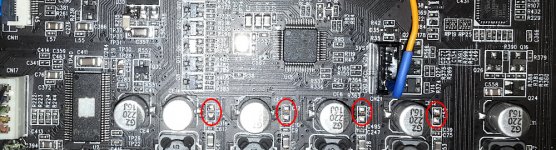
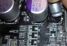
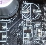
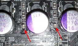
I was intrigued by the missing (unpopulated) ceramic caps beside these electrolytic filtering ones. These components were omitted to minimise the production costs. However, I appreciate these ceramic caps as important filtering devices, especially when about an SMPS output. I decided to repopulate the board with 0,1µ caps.
For those who may want do this mod, replacing these filtering caps, I may suggest to use quite near values (I used double values, and it works fine), to not load too much these small SMPSs, especially at the power up sequence. Too high capacities here may also increase the voltages on these outputs, which is not one will want at all...
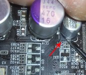
The biggest problem with this mod is to remove the old caps, without damaging the board`s traces/pads. I may suggest the follow (mechanical) procedure, which I tried it with success (after doing it by unsoldering on another board): Place a tool (very small screwdriver) on this side of the cap, as you see in the picture 1. Force carefully that side of the cap upward, until you feel it following your pushing force. Take out the screwdriver and move it back and forth in that same axe. After few such movements, push it again even more up, using the small screwdriver. Repeat the back and forth mouvements until it broke its legs. Do not use too much force in this operation, to prevent disclosing the cap together with the pads. Else the pads, are at normal temperature very solid glued on the board, and it tolerate very well this mechanical operation. Unsoldering operation it will disclose at once the pads and the traces. Not recommended at all!
Remove the rest og the cap`s legs with a low power soldering iron. That`s it!
Solder carefully the new good quality ones (lowest possible ESR) in place, the ceramic caps too, and be happy with the slightly improvement...
Most of the important improvements it come from other more complexe operations/directions...
BTW, the voltages at these outputs are under 6v, so 6v rated caps can be very well used here...
I was intrigued by the missing (unpopulated) ceramic caps beside these electrolytic filtering ones. These components were omitted to minimise the production costs. However, I appreciate these ceramic caps as important filtering devices, especially when about an SMPS output. I decided to repopulate the board with 0,1µ caps.
For those who may want do this mod, replacing these filtering caps, I may suggest to use quite near values (I used double values, and it works fine), to not load too much these small SMPSs, especially at the power up sequence. Too high capacities here may also increase the voltages on these outputs, which is not one will want at all...
The biggest problem with this mod is to remove the old caps, without damaging the board`s traces/pads. I may suggest the follow (mechanical) procedure, which I tried it with success (after doing it by unsoldering on another board): Place a tool (very small screwdriver) on this side of the cap, as you see in the picture 1. Force carefully that side of the cap upward, until you feel it following your pushing force. Take out the screwdriver and move it back and forth in that same axe. After few such movements, push it again even more up, using the small screwdriver. Repeat the back and forth mouvements until it broke its legs. Do not use too much force in this operation, to prevent disclosing the cap together with the pads. Else the pads, are at normal temperature very solid glued on the board, and it tolerate very well this mechanical operation. Unsoldering operation it will disclose at once the pads and the traces. Not recommended at all!
Remove the rest og the cap`s legs with a low power soldering iron. That`s it!
Solder carefully the new good quality ones (lowest possible ESR) in place, the ceramic caps too, and be happy with the slightly improvement...
Most of the important improvements it come from other more complexe operations/directions...
BTW, the voltages at these outputs are under 6v, so 6v rated caps can be very well used here...
Attachments
Last edited:
Isolated interface for USB board
I`m pleased to announce an quite important upgrade for 105/105D models: isolated interface for USB board. Now this device it is as it should on this area too. Its USB interface is now fully galvanic isolated from the rest.
A professional approach it will be available soon...
I`m pleased to announce an quite important upgrade for 105/105D models: isolated interface for USB board. Now this device it is as it should on this area too. Its USB interface is now fully galvanic isolated from the rest.
A professional approach it will be available soon...
My last USB board mod with the isolator in a quite prototype stage. A more professional edition of the isolator it will come soon...
The coax and Toslink interfaces on board, are disabled as follow this mod.
The coax and Toslink interfaces on board, are disabled as follow this mod.
Attachments
Last edited:
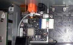
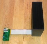
External LPM for 105/105D and 95 models
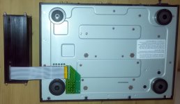
There is my approach for an external PSU for 105 and 95 models. The adaptor you see in the pictures, it fit for both 95/105, as the chassis pattern for perforations is the same. The sape of the perforations it differ, but my adaptor it fit in both cases. Shielded connection cables for main AC and toroid transformer are also included in this approach, but are not pictured. An similar light indicator, as on the players front panel (on/off - blue/red) it is also available on the front panel of the external LPM. Else no any other connections, but the flat cable.
I chosen the connection between the main flat cable and the adaptor, to be by screws terminal block, as this way it provide a better and much more ferm connection than a usual multi pins connector. At least the user may seldom need to connect or disconnect this external PSU, from the BD player.
After the adaptor is mounted in place, it need to be soldered for the contact pins. So this adaptor and its boards is to be permanent installed into device, and only connected or disconnected accordingly with the needs...
As one side of the LPM`s enclosure it is used as heatsink, the position of the box should be always vertical.
Attachments
Last edited:
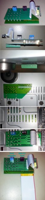
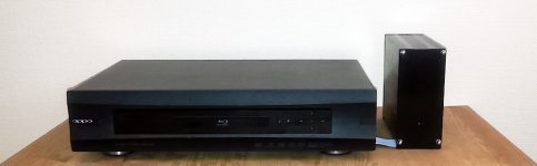
My external LPM approach. Here is pictured the 95 model, which is the main target for the concept, but it fit very well for 105/105D models, especially when the user need the multichannel board in place and functional.
Attachments
Last edited:
Experimenting with transformers...
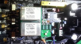
At least I was able to use my Lundahls 1684, I bought it for more than one year ago, as output stage for 105.
I have to admit that this approach is the simplest, very efficient and at least with the slightly better quality results, than my differential (active) output stage.
Using this passive stage for output, it simplify even more the whole modification approach for this player. There is no need any more of improved filtering or regulators for +/- power system on stereo board. With these transformers in place the only positive rail of this dual power system is used to power the mute relays (if the headphone chip is disabled/dismissed, as the rest of the original circuits). The general inside heat get lower. No any need for AC coupling on outputs, or improving of this stage.
The only modifications it still rest as necessary are the power system of the DAC chip, its clocking approach, as linking together the two differential outputs pairs available from the DAC (105 model). Then connect the transformers, and done!
I have experimented with different connection modes for the transformers (the known ones from these forum/threads). At least I chosen a quite simple connecting approach: the two DAC side windings in serial, and the output windings in serial too. Pure 1:1 as the transformer actually it is built for.
Comparing with my active differential stage, this passive one it give a lower output voltage (normal for such 1:1). I have 3,3Vpp on XLR outputs, instead of 5-6Vpp (active stage). This is not so big problem, as this almost 3dB level lose it can be easily compensated by the amplifier.
So far, so good...
The most interesting part of this experiment is the using of the (wide disputed) cap over DAC`s differential outputs. The effect of this cap it still apply very well in this transformer approach, as also Joe previously mentioned. As I want to keep the amplifying system`s gain as low as possible, I decided to not use a quite low signal level on the outputs in the Joe`s exposed approach. However, I mounted the cap over the DAC`s outputs, as I do it for my active differential stage. I used first the same value cap as for my module. It was wrong! A muffed sound, with well-increased low-end spectre, but strong attenuated high end. This attenuation it was perceived in a quite special way: a soundstage perceived as very far in space (far back from the speakers line). Else, the quality of the signal was not excessive altered... Well, something far from natural. I got lower in the caps value, and the results became better and better. I decided finally to use for moment 500pF film caps. I got a nice soundscene, wide, with good definition and resolution of the sound elements in space, as a very nice/deep low end spectre.
My conclusion so far about this cap approach: the cap value (the filter complex final value) is in connection, not only with the DAC output circuits approach, but also with the input impedance of the following circuit, whatever it may be: an opamp I/V stage or something different, as a passive stage (transformer). A quite large cap value is well working and is needed for that the improvement effect occur on the high impedance input of an active opamp stage, and a very low value for a very low input impedance as these transformers may have. This correlation it make sense as I can see so far. The main conclusion or confirmation here is that this cap approach it still working very well, and it do a good job.
As a conclusion, the transformers approach it have the advantages of a very simple solution, a slightly increasing in the output quality (comparing it with my active module), higher dynamics, and a superb result when using the right cap over the DAC`s outputs (transformers inputs). And another advantage, not to ignore it for these transformers pictured hereby: it fit very well in available space inside. Disadvantages: lower signal level (very easy to fix it), and maybe the price of the items (I have paid 250$ for two). In my opinion, the results it surpassing the disadvantages...
Using transformers on the ES9018 outputs is nothing new at all. I only want to confirm the very good results when using such approach.
Attachments
Last edited:
- Home
- Source & Line
- Digital Source
- Oppo's BDP105 - discussions, upgrading, mods...