The bootstrapped version probably comes with Prio 3-4, at the end.
I'll keep in mind to reserve a few nodes and sufficient real estate if at all possible.
No intention to try the high input Z before clarifying how to deal with aerial 50Hz and the neon lamps, WiFi, Bluetooth, 3G/5G etc.
I'll keep in mind to reserve a few nodes and sufficient real estate if at all possible.
No intention to try the high input Z before clarifying how to deal with aerial 50Hz and the neon lamps, WiFi, Bluetooth, 3G/5G etc.
I have tested the bootstrapped version, and it behaves exactly like in the sim: the input impedance is raised to several megohms, with a huge increase at ~1kHz (probably not 300 meg, but very high).
The circuit remains well-behaved in all conditions, including open-input, and the frequency response and distortion remain unaffected.
The circuit of post #116 should have a 12.35 kohm impedance minimum at 0.3228687 Hz, if I calculated it correctly. Admittedly, that is very far in the subsonic region.
Half a dozen additional nodes compared to a transistor or 317 follower?to just stay simple
Yes, just half a dozen more. Anyway, it's for Ionmw to decideLooks about the same number of nodes as the 317 follower?
Not only about nodes count but also component count around each node. Then the parts which are in series, not forming a node but needing traces and holes.
Apparently, the Post #126 proposal compares itself to the bootstrapped version of 317.
My current plan is to keep the 317 basic and simple, only with improved PSRR. I will try keeping the possibility for bootstrapping for the end: but optional.
If else, a true 1-BJT still suits the LineOut purpose (but Headphones derivation will be removed).
Then again, the 317 fits excellent the requirements for Line out with Phones derivation. I am replacing a 3-BJT LineOut former schematic with 1-BJT footprint.
So, if I want to unnecessarily go back to 3-BJT then I would not need to change the old schematic/PCB at all. Right?
Neh overall but thank you for insight and interesting proposal. Topic remains to use only a 1-BJT footprint for LineOut (and use the remaining 2-BJT footprints for other functions, without need to go invasive in the PCB). No change means: bridges are allowed but new holes or old traces cutting are not. Also, proper layout.
It is highly focused on wishes and it is specific to the PCB in hand.
Will share the photos and more details (the off topic ones) when the mod is fully ready, tested and approved by me and some friends with good ears (which can detect by listening tests if my solution is not faulty).
On the other hand, if a new PCB would be in Scope, then to choose one schematic from >100 possibilities is destined to be anyway a niche solution")
Will share the photos and more details (the off topic ones) when the mod is fully ready, tested and approved by me and some friends with good ears (which can detect by listening tests if my solution is not faulty).
On the other hand, if a new PCB would be in Scope, then to choose one schematic from >100 possibilities is destined to be anyway a niche solution
I think, my approach to make it the simplest possible way (but not too simple, as listening to experts is always only helpful) is professional and elegant.
I always liked the rare situations when properly talking&listening to real experts transforms a 2K€-5K€ product into a 20€ Product with the same performance as the original and more. In this case is not a 2K-5K product, but still long-time wishes will be fulfilled and pleasure will be present
I always liked the rare situations when properly talking&listening to real experts transforms a 2K€-5K€ product into a 20€ Product with the same performance as the original and more. In this case is not a 2K-5K product, but still long-time wishes will be fulfilled and pleasure will be present
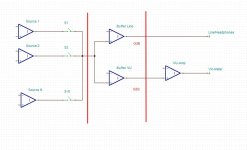
Plan is the following.
Ideally the VU-amp is to be connected at 'Buffer Line' output (so, have one single Buffer). If VU-amp does not make the Line-Out dirty (reverse isolation >90dB).
If not possible, then I need a second buffer, for VU derivation.
Ideally the VU-amp is to be connected at 'Buffer Line' output (so, have one single Buffer). If VU-amp does not make the Line-Out dirty (reverse isolation >90dB).
If not possible, then I need a second buffer, for VU derivation.
Attachments
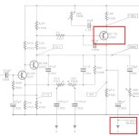
In particular, I copy the VU-amp from Revox A77 (Recamp card):
- theory & praxis tells, that if they could put it there, directly in the heart of the REC Preamp/EQ (no buffer involved), then it should have no back-feeding into the EQ node.
So, I should be able to connect the VU-amp input to the LineOut buffer.
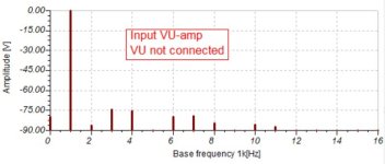
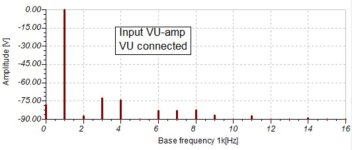
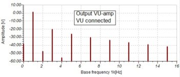
Momentarily this does not happen: I am testing without buffer, simply after Selector switch. VU-meter works fine and is correctly calibrated, but I observe quite an impact at the VU-Amp input (back isolation poor). Indicates that it will impact the signal Line Out, making it dirty.
As written at beginning of this thread, I suspect this is an effect impedance mismatch effects. I need to put buffers (find&allocate 1-BJT footprints for each of them).
On the other hand, I do not see why Revox implementation is innocent but mine is wrong. Of course I do not like to waste a second buffer only for VU.
- theory & praxis tells, that if they could put it there, directly in the heart of the REC Preamp/EQ (no buffer involved), then it should have no back-feeding into the EQ node.
So, I should be able to connect the VU-amp input to the LineOut buffer.
Momentarily this does not happen: I am testing without buffer, simply after Selector switch. VU-meter works fine and is correctly calibrated, but I observe quite an impact at the VU-Amp input (back isolation poor). Indicates that it will impact the signal Line Out, making it dirty.
As written at beginning of this thread, I suspect this is an effect impedance mismatch effects. I need to put buffers (find&allocate 1-BJT footprints for each of them).
On the other hand, I do not see why Revox implementation is innocent but mine is wrong. Of course I do not like to waste a second buffer only for VU.
Attachments
what I can note:
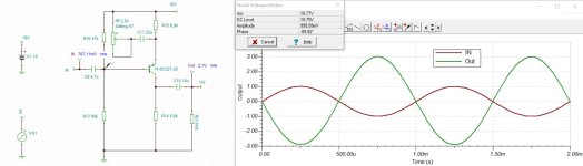
Having R507, C508 and P504 (non zero position) implemented, the reverse isolation is still equally poor.
I suspect that in reality the source impedance is not zero as in the simulations... ? Could this explain the case?
I also measure(!) that source output is still correct 0dB but Vu-amp input is like -20dB. I t should be a direct connection, but apparently is not.
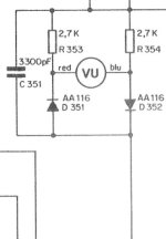
- I did not use R507 (1KOhm)
- also C508 (180pF) not used
- the P504 (500Ohm) simulates good with 1.2KOhm value, but in reality the best VU-calibration I could obtain was with 0 Ohm (short).
Having R507, C508 and P504 (non zero position) implemented, the reverse isolation is still equally poor.
I suspect that in reality the source impedance is not zero as in the simulations... ? Could this explain the case?
I also measure(!) that source output is still correct 0dB but Vu-amp input is like -20dB. I t should be a direct connection, but apparently is not.
please exemplify visually, to be fully clear.how about using a jfet/mosfet input for isolation?
- Home
- Source & Line
- Analog Line Level
- One BJT line amp/buffer