Just curious why you're using the OPA827 instead of the OPA627?
Do you think the '827's SQ is as good as the '627's?
Good question! Mainly cost. For the parameters that matter for audio I think the OPA827 does about 90% of the OPA627 for 60% less money per chip. Those OPA627s are still clocking in at around $25 each, even for the lowest grade, at Mouser vs. $10 for the OPA827.
There is some functionality in the OPA627 we would be paying for but don't need too. Double the slew rate is one. The OPA827 is already around 20V/uS and I think the 627 was about double that. Inserted into the O2 the whole thing will be limited to just 6V/uS by that gain stage NJM2068 chip. The O2's original NJM4556As that the Booster replaces are just 3V/uS.
Another is the input offset voltage. The best grade of the 627 is 40uV to 100uV, while the 827 is 75uV to 150uV from the respective data sheets. One of my big goals with the Booster Board was to dramatically lower the output DC offset vs. the 3600uV or so of the stock O2. Initially I figured that the 75uV to 150uV was good enough, given the huge price difference vs. the 627. But in actual practice since then, after measuring dozens of these things built up with the 827, I'm pleased to say I haven't measured a single one that has been more than 55uV. I just measured a new Booster Board a few minutes ago (different one than the tests above) and I found 45uV on one channel and 4uV on the other.
The input voltage noise graph of the 827 is slightly better. It doesn't look like it at first, the way the two datasheets have it drawn. First page of the 827 sheet and fig 1 in the 627 sheet. They ran the vertical axis up to 1000 nV/sqrt(Hz) on the 627 sheet so the curve looks compressed. Check out the point where the two graphs cross the 10nV/sqrt(Hz) line. For the 827 it is around 4Hz, while the 627 is around 30Hz. But even here those frequencies are so low the difference probably isn't audible.
The THD+N graph of the 627 is just very slightly better. But there I figured the THD+N of the O2 gain stage may very well swamp that much of a decrease. That would be an interesting thing to measure with an AP!
On the flip side, the OPA627 shouldn't make anything worse, and may be a fun chip to try! I haven't actually soldered a pair of 627s into the recent versions of the Booster Board to check for oscillations though, but I would be surprised if there was a problem. The GBW of the two chips is about the same.
One other interesting bit of chip history on the Booster Board. My original intent was to use the OPA140, from a good suggestion by Sergey888. It is even cheaper and has similar very good specifications, plus very low idle current to be battery-friendly. I've found one glitch though that makes me nervous. The output impedance shoots up dramatically below 1KHz, from one of the datasheet graphs. I wasn't sure if the negative feedback around the composite pair would zero that out, as it does with the "outer" LME49600 buffer chip. johnc124 answered that for me a few months ago, it doesn't. Even then it *shouldn't* make a difference, given that all the chip is powering is the input impedance of the LME49600 chip. Lol, yet another thing that would be interesting to check with an AP. That one parameter spooked me enough to switch the standard chip in the BOM over to the OPA827 a few versions ago.
Last edited:
Thank you for the detailed reply!
I've never heard of nor tried the OPA140/2140.
Do you mean its output impedance goes up drastically under a load?
If trying to use it within the feedback loop of another op-amp, do you think that would still be a problem?
If so, I think I'll pass on ordering any.
I've never heard of nor tried the OPA140/2140.
Do you mean its output impedance goes up drastically under a load?
If trying to use it within the feedback loop of another op-amp, do you think that would still be a problem?
If so, I think I'll pass on ordering any.
johnc124 answered that for me a few months ago, it doesn't. Even then it *shouldn't* make a difference, given that all the chip is powering is the input impedance of the LME49600 chip. Lol, yet another thing that would be interesting to check with an AP.
Why don't you send tomchr a booster board with an opa2140 on one channel and an opa827 on the other??... 😀
Last edited:
Why don't you send tomchr a booster board with an opa2140 on one channel and an opa827 on the other??... ��
WOW!! I like it! Good suggestion.
") Here is an opportunity to find out how the OPA140 compares with the OPA827, at least in this duty as a composite with the LME49600.
Here is an opportunity to find out how the OPA140 compares with the OPA827, at least in this duty as a composite with the LME49600.Do you mean its output impedance goes up drastically under a load?
If trying to use it within the feedback loop of another op-amp, do you think that would still be a problem?
The open-loop output Z shoots up vs. frequency. It is figure 18 in the OPA140 datasheet:
http://www.ti.com/lit/gpn/opa2140 (opens PDF)
So the output Z stays around 10 ohms from 1KHz to 100KHz. But below 1KHz it shoots way up to 700 ohms at 10Hz!
Now compare that to the same curve on the OPA827 sheet, figure 27:
http://www.ti.com/lit/gpn/opa827 (opens PDF)
Completely flat at 20 ohms, from 100Hz out to 4MHz. Probably reasonable to extrapolate that being flat out to 10Hz, even though it isn't shown
Now if the chip was being used just as a single stage the negative feedback would take care of most or all of the internal Z. But with the composite amplifier here, the OPA140 in a loop with the LME49600, johnc124 confirmed for me (I never could quite get my arms around it) that while the overall negative feedback does zero out the internal Z of the output chip, as we all expect, it doesn't for the "inner" driving chip. I'm assuming it would take a multiloop configuration then to do that, if needed, something like this in one of Tangent's designs:
http://tangentsoft.net/audio/pimeta2/misc/sch-2.01.pdf (opens PDF)
But.. all that "inner" composite chip is driving is the input impedance of the LME49600. I believe I've tried to find that number before, for either the LME49600 or BUF634, and no luck. But I'll guess no more than 1nF, which would be a corner frequency with the 700 R of 220KHz, if I've done that right, which wouldn't be a problem. So I'm thinking it is a non-issue, at least for the composite amp, but the answer for that is above my pay grade.
CHiroshi's suggestion above should answer the question. Build up the other channel of the Booster with the OPA140 and see how that compares in the AP testing to the OPA827. The results would be extremely interesting!
Last edited:
By using one OP140 and a OP827...in the booster board would this in anyway add to or create any issues?? Being a purist wouldn't it be "better?" to have both the same for measurements...ie like used in the real world??
Then do one with the other op amp?. Send Tom the op amps??? easy to pop in etc??
Alex
:>)
Then do one with the other op amp?. Send Tom the op amps??? easy to pop in etc??
Alex
:>)
easy to pop in etc??
SOICs are not "easy to pop in".
WOW!! I like it! Good suggestion.
I know, it's genius! 😉
I'm a professional musician, and a hobby sound engineer in my spare time, kinda used to think in terms of recording tracks! 😎🎹
Last edited:
I'm in no way an electrical engineer, but electrically it shouldn't make a difference. If anything, the power supply will be loaded unevenly, but the rails are shared anyways so...By using one OP140 and a OP827...in the booster board would this in anyway add to or create any issues?? Being a purist wouldn't it be "better?" to have both the same for measurements...
:>)
Agdr, correct me if I'm talking sh*t!...
Good thoughts! The Booster Board wound up as "dual mono" with completely separate sections, other than the common power supply. Using a different chip for one channel shouldn't affect the other, luckily. There might be some small differences between the channels, especially in very low level (inaudible, below -120dB) noise due to the proximity of the connection pins on one channel to the O2 power supply filter capacitors, but not in THD due to the symmetry.
Interesting history on that one too from earlier in the thread. I was debating about using a dual op-amp vs. two singles. At the time the OPA2140 was announced but wasn't shipping yet, just the single OPA140. I also wanted to leave open the possibility of using the OPA827 and OPA627 which are only available as singles. So two single chips won, even though it resulted in more parts.
Wouldn't it be something if the OPA140 turns out to be nearly indistinguishable in this application from the OPA827 in the AP measurements? The 140s are going for $5, half the cost of the 827s, plus they have half the idle current.
This probably means I need to have tomchr run a frequency response test too, which I was going to leave out. I'm slowly compiling a list of tests for him to quote the cost.
Interesting history on that one too from earlier in the thread. I was debating about using a dual op-amp vs. two singles. At the time the OPA2140 was announced but wasn't shipping yet, just the single OPA140. I also wanted to leave open the possibility of using the OPA827 and OPA627 which are only available as singles. So two single chips won, even though it resulted in more parts.
Wouldn't it be something if the OPA140 turns out to be nearly indistinguishable in this application from the OPA827 in the AP measurements? The 140s are going for $5, half the cost of the 827s, plus they have half the idle current.
This probably means I need to have tomchr run a frequency response test too, which I was going to leave out.
I'm slowly compiling a list of tests for him to quote the cost.
Last edited:
Your probably right, but as a simple ET, there may be some differences in slew rate etc that might affect the sound? Most likely imperceptible.
I would hate to send this to Tom and pay for results that "might" be in question.
AGDR will most likely know...
Alex
ooops again just saw AGDR's post!
I would hate to send this to Tom and pay for results that "might" be in question.
AGDR will most likely know...
Alex
ooops again just saw AGDR's post!
Hmm.... I could certainly send Tom two amps! I have a bunch of O2 boards, parts, cases, and now bare Booster Boards after this last run. I'll ponder that.
I could ship off one amp assembled with OPA827s on the Booster and another with OPA140s, then ask Tom to measure the same channel on each for the THD+N test. Then there wouldn't be any question it was an apples-to-apples comparison on the two chips.
Then one thing I could try then is to use a different LME49600 bandwidth resistor on the other channel on the OPA140 board and measure that. With the V3.6 I've gone to using a mid-range BW resistor for each buffer as the BOM default rather than the prior none at all (mid-BW rather than low-BW), 750R. I could try 100R for "high bandwidth" on the other channel. According to the LME49600 data sheet, as I recall, in addition to stability with some op-amps the higher-quiescent "high BW" mode has slightly better THD. I'll have to go back and review the sheet through, I might be mixing that up with just swapping out with the now-unobtainable LME49610.
BTW, I'm not aware of any stability issues, but if someone wants to mod their prior V3.5 boards for mid-BW on the buffer chips the pads are there, the two 0805 sized pads near the LME49600s. A little tricky to solder the one in the middle after the LME49600s are in, but possible since I did it on one board here. You would use Mouser #754-RG2012P-751-B-T5, or just drop me a PM and I'll put one in a letter envelope, no charge. Going mid-BW pulls an additional 4mA per buffer chip and generates an additional 100mW in idle heat per buffer chip vs. the prior low-BW, both insignificant.
Shipping would probably be the same too in both directions too in sending Tom two amps for test, I'll probably use the USPS medium flat rate box.
I could ship off one amp assembled with OPA827s on the Booster and another with OPA140s, then ask Tom to measure the same channel on each for the THD+N test. Then there wouldn't be any question it was an apples-to-apples comparison on the two chips.
Then one thing I could try then is to use a different LME49600 bandwidth resistor on the other channel on the OPA140 board and measure that. With the V3.6 I've gone to using a mid-range BW resistor for each buffer as the BOM default rather than the prior none at all (mid-BW rather than low-BW), 750R. I could try 100R for "high bandwidth" on the other channel. According to the LME49600 data sheet, as I recall, in addition to stability with some op-amps the higher-quiescent "high BW" mode has slightly better THD. I'll have to go back and review the sheet through, I might be mixing that up with just swapping out with the now-unobtainable LME49610.
BTW, I'm not aware of any stability issues, but if someone wants to mod their prior V3.5 boards for mid-BW on the buffer chips the pads are there, the two 0805 sized pads near the LME49600s. A little tricky to solder the one in the middle after the LME49600s are in, but possible since I did it on one board here. You would use Mouser #754-RG2012P-751-B-T5, or just drop me a PM and I'll put one in a letter envelope, no charge.
Going mid-BW pulls an additional 4mA per buffer chip and generates an additional 100mW in idle heat per buffer chip vs. the prior low-BW, both insignificant.Shipping would probably be the same too in both directions too in sending Tom two amps for test, I'll probably use the USPS medium flat rate box.
Last edited:
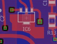
IC5 is now IC6 on V3.6
It has just been brought to my attention that on the new V3.6 boards the prior IC5 is now labelled IC6. There is no IC5 anymore. I've changed the part number on the BOM and just re-uploaded. The link is in the first post in this thread.
When soldering that part I recommend doing it just as with the LME49600 buffers. I first put a very thin layer of solder on the PC heat sink area, then a thin layer on the back of the part. Put the part in place holding it on the sides with tweezers and heat up the back of the metal tab, to melt the solder. Reheat as necessary to line the pins in front up with their PCB pads. Then reheat one more time while pressing down on the part to make sure it sits flat on the board. Finally go ahead and solder up the pins in front, but you only need to solder the two outer pins since the center pin is attached to the heat sink.
Attachments
Last edited:
Suggested O2 IC sockets when using the Booster Board
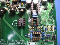
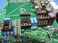
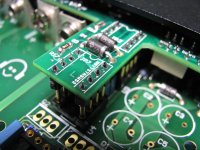
If an O2 PC board is being built up specifically for use with the Booster Board, I would suggest using collet IC sockets instead of the flat blade sockets that NwAvGuy has in the O2 BOM. The collet sockets make it easy to get the connection pins centered. The Booster works great with the regular (O2 BOM) sockets, you just have to do a little extra inspection to make sure the connection pins are centered in the middle of the flat socket blades, as shown below.
The sockets to use are Mouser #575-113308 (Digikey #ED56083-ND), which are Mill Max #110-13-308-41-001000, or an alternate socket at Digikey is #ED3013-ND, which are On Shore Tech #SA083040. You need a total of 4, of course, for the O2 PC board. I'm going to add these to a new section at the bottom of the Booster Board BOM today and re-upload it at the Google Drive link.
Below are some photos.
* In the first two I've built up an O2 PC board with the new sockets. Some of the taller O2 parts are left off here to get a good look at the sockets. I've set one of the old flat-blade sockets (from the O2 BOM) there for comparison. In that first photo note that there is no question about alignment with the collet sockets, but with the flat blade sockets you have 1mm of wiggle room front to back. With an IC it wouldn't matter where it sits in the socket, but with the Booster connection pins you want to get the centered in the middle of those flat blades.
The second photo shows a set of connection pins plugged into one of the sockets. ICs fit just fine in the collet sockets too, of course.
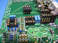
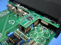
* The next 2 photos are a close-up of the connection pins being inserted into the collet sockets.
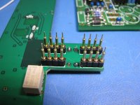
* The next 2 show the Booster Board being placed over the connection pins, then slid half way into an O2 case. As per the build instructions I recommend sliding the boards into a case like this to insure they are perfectly lined up while soldering the pins.
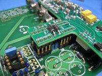
* In the next photo, a sideways look through the connection pins, note how the 2 rows in front line up left-to-right with the 2 in back. They don't really have a choice when using the collet IC sockets, but when using the flat blade IC sockets you need to look through the pins like this and adjust the front and back rows in the sockets to make sure they line up.
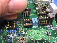
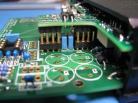
* The final 2 photos show the results with the connection pins soldered up. Note that the black plastic bar on the connection pins goes up, toward the Booster Board, as per the build instructions.
Remember you can click on the arrows in the lower left corner of the photos to zoom them up.
If an O2 PC board is being built up specifically for use with the Booster Board, I would suggest using collet IC sockets instead of the flat blade sockets that NwAvGuy has in the O2 BOM. The collet sockets make it easy to get the connection pins centered. The Booster works great with the regular (O2 BOM) sockets, you just have to do a little extra inspection to make sure the connection pins are centered in the middle of the flat socket blades, as shown below.
The sockets to use are Mouser #575-113308 (Digikey #ED56083-ND), which are Mill Max #110-13-308-41-001000, or an alternate socket at Digikey is #ED3013-ND, which are On Shore Tech #SA083040. You need a total of 4, of course, for the O2 PC board. I'm going to add these to a new section at the bottom of the Booster Board BOM today and re-upload it at the Google Drive link.
Below are some photos.
* In the first two I've built up an O2 PC board with the new sockets. Some of the taller O2 parts are left off here to get a good look at the sockets. I've set one of the old flat-blade sockets (from the O2 BOM) there for comparison. In that first photo note that there is no question about alignment with the collet sockets, but with the flat blade sockets you have 1mm of wiggle room front to back. With an IC it wouldn't matter where it sits in the socket, but with the Booster connection pins you want to get the centered in the middle of those flat blades.
The second photo shows a set of connection pins plugged into one of the sockets. ICs fit just fine in the collet sockets too, of course.
* The next 2 photos are a close-up of the connection pins being inserted into the collet sockets.
* The next 2 show the Booster Board being placed over the connection pins, then slid half way into an O2 case. As per the build instructions I recommend sliding the boards into a case like this to insure they are perfectly lined up while soldering the pins.
* In the next photo, a sideways look through the connection pins, note how the 2 rows in front line up left-to-right with the 2 in back. They don't really have a choice when using the collet IC sockets, but when using the flat blade IC sockets you need to look through the pins like this and adjust the front and back rows in the sockets to make sure they line up.
* The final 2 photos show the results with the connection pins soldered up. Note that the black plastic bar on the connection pins goes up, toward the Booster Board, as per the build instructions.
Remember you can click on the arrows in the lower left corner of the photos to zoom them up.
Attachments
-
 IMG_4930.JPG779.9 KB · Views: 260
 -
 IMG_4931.JPG670.3 KB · Views: 250
 -
 IMG_4932.JPG640.2 KB · Views: 245
 -
 IMG_4933.JPG679.9 KB · Views: 237
 -
 IMG_4936.JPG657.3 KB · Views: 121
 -
 IMG_4935.JPG692.7 KB · Views: 121
 -
 IMG_4937.JPG573.8 KB · Views: 111
 -
 IMG_4938.JPG598.9 KB · Views: 115
 -
 IMG_4939.JPG580.6 KB · Views: 134
Last edited:
QA401 noise floor tests, AC and batteries, OPA140 & OPA827
I've finally had a chance to build up two O2 + V3.6 booster boards, with one Booster using OPA140 chips and the other OPA827 chips. I'm going to use tomchr's consulting service to do some AP tests in a month or two, but first wanted to do a set of tests with the QA401 to compare. I'm trying to replicate what NwAvGuy did with his dScope O2 testing here:
NwAvGuy: O2 Headphone Amp (scroll down)
The noise floor graphs are the 2nd down, on batteries, and the 4th down, on AC. At the bottom of all the graphs he says he used the 16Vac 500mA Triad transformer, so that is what I'm using here.
He also apparently left his dScope plugged into the O2 input for noise floor, because he specifies 25R input impedance which at the bottom says is the output impedance of the dScope. No idea why he didn't just leave the O2 inputs shorted, which would be the more typical way to do it. So to get apples-to-apples I've made a up 3.5mm plug with 2 25 ohm, 0.1%, metal film, 25 PPM/C resistors inside (metal shell), Mouser #71-RN55E25R0B. I've also done tests with the input shorted. I won't post those here but all the tests will be up at the project Google Drive link.
The O2 boards are built up exactly from NwAvGuy's BOM, except with the following part upgrades from my website:
C1, C6, C7 dielectric upgraded to X7R from the BOM's Y5V. The cap value & voltage remains the same. These are not in the audio path.
C2-C5 filter capacitors upgraded to his BOM's alternate choice listing of panasonic 667-EEUFR1V471B. Half the ESR, twice the ripple current, and 105C vs. 85C given that C5 nearly touches one of the O2 voltage regulators.
R14 & R20 changed to the SFR series to match his other audio-path resistor choices (Mouser didn't stock this one in SFR but Digikey does)
C16 and C21 - dielectric upgraded to X7R from Z5U. Tolerance upgraded to 5% from 20%. Same capacitance and voltage. These are not in the audio path.
The lower noise DD version of the NJM2068 chip is used.
Batteries are the original 250mAhr Tenergy NiMH.
I've increased the size of the power jack panel hole to 11/32" (8.73mm) to allow the plastic molding on the power plug to go through, insuring the metal barrel of the power jack doesn't touch the metal panel side.
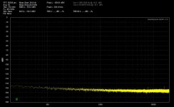
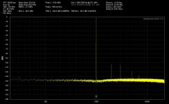
On batteries
The test conditions then are exactly what NwAvGuy lists in the 2nd graph down: on batteries, 2.5x gain, 25R source impedance, volume 100%, dBV.
The first graph is the OPA140 booster board, the second the OPA827. Both are the left O2+Booster channels. I tested both channels and no significant difference from left to right. I'll post both tests on the Google Drive link.
So the OPA827 Booster Board comes in a just a hair lower noise floor than NwAvGuy's O2 battery tests, at -112.3dBV vs. -111.9dBV. The OPA140 version of the Booster has a noise floor 2dBV higher at -110.4dBV. BUT... take these with a grain of salt, because it is the QA401 at the bottom of its noise floor, not an AP. At least in terms of absolute value, the relative values here probably are of some use, ie that the OPA140 is a tiny 2dBV noisier than the OPA827. The OPA827 is twice the price so hopefully there is some additional value like this! But again, at noise levels this small, they are not likely to be audible. An argument could be made that the OPA140 actually wins, given the lower price even if it is 2dBV nosier.
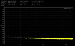
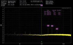
On AC
Same thing as above, but now with the 16Vac 500mA transformer that NwAvGuy used. Same test conditions as his 4th graph: on AC, 2.5x gain, 25R source impedance, volume 100%, dBV.
The first graph is the OPA140 booster board, the second the OPA827. Both are the left O2+Booster channels. I tested both channels and no significant difference from left to right. I'll post both tests on the Google Drive link.
The small amount of AC 60Hz now shows up, in the -140dBV range, same as NwAvGuy's measurements. Here both the OPA827 and OPA140 come out about the same at -110.4dBV, which I take to mean the powerline at 60Hz is the largest component of the noise floor spectrum. That is vs. the same -111.9dBV for NwAvGuy's AC test.
Results
Since this is the QA401 and not an AP I wouldn't read too much into anything being "better" than the stock O2. I'll leave that to the actual AP testing with tomchr in a month or two. The important thing here to me is that the Booster Board, with either the OPA140 or OPA827 chips, apparently doesn't make the noise floor significantly any worse than the stock O2. The Booster is replacing the single NJM4556A chip on each channel with 2 chips, the OPAxxx + LME49600 composite pair, plus there are Booster Board parts in proximity to the AC supply area of the O2. So the potential was there for some increased noise over the stock O2. Not so from these tests.
Said another way, the Booster provides benefits from increased peak current, vastly lower DC output offset, headphone relay, and possibly lower THD (to be tested). So for noise floor here, simply not being worse than the stock O2 is a "win" in my view. I've made the comment to tomchr in an email that if the noise floor testing showed a problem the rest would probably be moot until the problem was fixed.
I've finally had a chance to build up two O2 + V3.6 booster boards, with one Booster using OPA140 chips and the other OPA827 chips. I'm going to use tomchr's consulting service to do some AP tests in a month or two, but first wanted to do a set of tests with the QA401 to compare. I'm trying to replicate what NwAvGuy did with his dScope O2 testing here:
NwAvGuy: O2 Headphone Amp (scroll down)
The noise floor graphs are the 2nd down, on batteries, and the 4th down, on AC. At the bottom of all the graphs he says he used the 16Vac 500mA Triad transformer, so that is what I'm using here.
He also apparently left his dScope plugged into the O2 input for noise floor, because he specifies 25R input impedance which at the bottom says is the output impedance of the dScope. No idea why he didn't just leave the O2 inputs shorted, which would be the more typical way to do it. So to get apples-to-apples I've made a up 3.5mm plug with 2 25 ohm, 0.1%, metal film, 25 PPM/C resistors inside (metal shell), Mouser #71-RN55E25R0B. I've also done tests with the input shorted. I won't post those here but all the tests will be up at the project Google Drive link.
The O2 boards are built up exactly from NwAvGuy's BOM, except with the following part upgrades from my website:
C1, C6, C7 dielectric upgraded to X7R from the BOM's Y5V. The cap value & voltage remains the same. These are not in the audio path.
C2-C5 filter capacitors upgraded to his BOM's alternate choice listing of panasonic 667-EEUFR1V471B. Half the ESR, twice the ripple current, and 105C vs. 85C given that C5 nearly touches one of the O2 voltage regulators.
R14 & R20 changed to the SFR series to match his other audio-path resistor choices (Mouser didn't stock this one in SFR but Digikey does)
C16 and C21 - dielectric upgraded to X7R from Z5U. Tolerance upgraded to 5% from 20%. Same capacitance and voltage. These are not in the audio path.
The lower noise DD version of the NJM2068 chip is used.
Batteries are the original 250mAhr Tenergy NiMH.
I've increased the size of the power jack panel hole to 11/32" (8.73mm) to allow the plastic molding on the power plug to go through, insuring the metal barrel of the power jack doesn't touch the metal panel side.
On batteries
The test conditions then are exactly what NwAvGuy lists in the 2nd graph down: on batteries, 2.5x gain, 25R source impedance, volume 100%, dBV.
The first graph is the OPA140 booster board, the second the OPA827. Both are the left O2+Booster channels. I tested both channels and no significant difference from left to right. I'll post both tests on the Google Drive link.
So the OPA827 Booster Board comes in a just a hair lower noise floor than NwAvGuy's O2 battery tests, at -112.3dBV vs. -111.9dBV. The OPA140 version of the Booster has a noise floor 2dBV higher at -110.4dBV. BUT... take these with a grain of salt, because it is the QA401 at the bottom of its noise floor, not an AP. At least in terms of absolute value, the relative values here probably are of some use, ie that the OPA140 is a tiny 2dBV noisier than the OPA827. The OPA827 is twice the price so hopefully there is some additional value like this!
But again, at noise levels this small, they are not likely to be audible. An argument could be made that the OPA140 actually wins, given the lower price even if it is 2dBV nosier.On AC
Same thing as above, but now with the 16Vac 500mA transformer that NwAvGuy used. Same test conditions as his 4th graph: on AC, 2.5x gain, 25R source impedance, volume 100%, dBV.
The first graph is the OPA140 booster board, the second the OPA827. Both are the left O2+Booster channels. I tested both channels and no significant difference from left to right. I'll post both tests on the Google Drive link.
The small amount of AC 60Hz now shows up, in the -140dBV range, same as NwAvGuy's measurements. Here both the OPA827 and OPA140 come out about the same at -110.4dBV, which I take to mean the powerline at 60Hz is the largest component of the noise floor spectrum. That is vs. the same -111.9dBV for NwAvGuy's AC test.
Results
Since this is the QA401 and not an AP I wouldn't read too much into anything being "better" than the stock O2. I'll leave that to the actual AP testing with tomchr in a month or two.
The important thing here to me is that the Booster Board, with either the OPA140 or OPA827 chips, apparently doesn't make the noise floor significantly any worse than the stock O2. The Booster is replacing the single NJM4556A chip on each channel with 2 chips, the OPAxxx + LME49600 composite pair, plus there are Booster Board parts in proximity to the AC supply area of the O2. So the potential was there for some increased noise over the stock O2. Not so from these tests.Said another way, the Booster provides benefits from increased peak current, vastly lower DC output offset, headphone relay, and possibly lower THD (to be tested). So for noise floor here, simply not being worse than the stock O2 is a "win" in my view.
I've made the comment to tomchr in an email that if the noise floor testing showed a problem the rest would probably be moot until the problem was fixed.Attachments
Last edited:
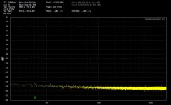
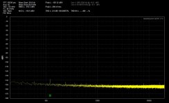
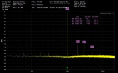
QA401 THD+N tests into 15R and 600R loads, OPA827 & OPA140
Here is a round of THD+N tests with the QA401 on an O2 + Booster Board built with the OPA827 and a different one built with OPA140 chips. These are done with 15R and 600R loads. I've been especially interested in the 15R load to compare with NwAvGuy's dScope tests of the O2 into 15R, the 18th graph he posted here:
NwAvGuy: O2 Headphone Amp (scroll down)
I *think* it is beating the pants off the stock O2 here. The 15R test load resistor is a non-inductive 5W 1% 20PPM/C, Mouser #588-WNE15RFET. The 600R is Mouser #71-PTF56600R00BZEK, 0.1%, 1/8W, 5 PPM/C/
NwAvGuy's test conditions are on AC, with the 16Vac 500mA transformer, Vol=100% and BW=22KHz. The tests here match all of these. Where it gets a bit complicated is he used dBr, relative to 400mB. Here I'm using 0dBV, 1Vrms. He says to convert subtract 8dB from the dBV to get the 400mV dBr. I believe that is correct.
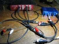
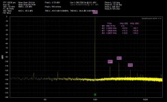
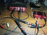
The graphs below are into 15R on AC and into 600R on batteries with the OPA827 Booster Board (blue case). The 3rd graph is the loopback of the QA401 at 0dBV. The next 2 are the test setup.
Comparing the 15R THD plot here with "THD+N 15 Ohms spectrum" in his 18th graph, the numbers are substantially below (better). Then subtract off 8dB for dBV-to-dBr and they get even better. Then subtract out the inherent 2nd and 3rd harmonics in the QA401 in that loopback plot and thet get better still. And finally, with regards to THD+N, this is a cheap QA401 vs. his dScope so the actual noise floor is likely less than it comes up with here.
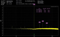
The next 2 graphs are the same 15R and 600R loads with the Booster Board built up with OPA140 chips, and the final photo the OPA140 test setup. Note that the OPA827 and OPA140 results into the two loads are nearly identical! The OPA140 even appears just a tiny bit better, but within error bars here. So far it does look like the OPA140 is a viable chip for the Booster. It costs half as much and has half the idle current. Again credit were credit is due, Sergey888 was the one who mentioned that chip way back when. I hadn't heard of it before. I still need to run a frequency response test to verify that increase in output Z the 140 has doesn't matter here.
Here is another fun thing you can do with the numbers in these plots. Up at the top in the middle of the QA401 graphs the QA401 lists the measured output voltage of the Booster Board in mV(rms). For the 600 ohm load it shows 961mV(rms) while for the 15R load it shows 918mV(rms). Well there is your output impedance of the Booster Board, that additional internal voltage drop! Remember that the stock O2 output 1R balancing resistors are left in place on these boards (but can be jumpered, the Booster doesn't need them). So that is 1R || 1R = 0.5R, the output Z of the O2.
The current through the 15R load resistor would be 918mV(rms)/15R = 61mA(rms). Assuming the 600R voltage is close to the no-load voltage, the voltage across the internal Z is .961 - .918 = .043mV(rms). The Booster output Z is therefore .043mV(rms)/.061mA(rms) = 0.7R. Close to the 0.5R! Close enough to be a double check. That remaining 0.2R is likely test lead resistances and the 600R being slightly different from no-load.
From these graphs the Booster Board appears to have substantially less THD than the stock O2 NJM4556A chips, from the NwAvGuy graph, into low impedance loads. Once tomchr does a more official Booster Board test here on his AP in a month or so it will be interesting to compare with these QA401 results.
Here is a round of THD+N tests with the QA401 on an O2 + Booster Board built with the OPA827 and a different one built with OPA140 chips. These are done with 15R and 600R loads. I've been especially interested in the 15R load to compare with NwAvGuy's dScope tests of the O2 into 15R, the 18th graph he posted here:
NwAvGuy: O2 Headphone Amp (scroll down)
I *think* it is beating the pants off the stock O2 here.
The 15R test load resistor is a non-inductive 5W 1% 20PPM/C, Mouser #588-WNE15RFET. The 600R is Mouser #71-PTF56600R00BZEK, 0.1%, 1/8W, 5 PPM/C/NwAvGuy's test conditions are on AC, with the 16Vac 500mA transformer, Vol=100% and BW=22KHz. The tests here match all of these. Where it gets a bit complicated is he used dBr, relative to 400mB. Here I'm using 0dBV, 1Vrms. He says to convert subtract 8dB from the dBV to get the 400mV dBr. I believe that is correct.
The graphs below are into 15R on AC and into 600R on batteries with the OPA827 Booster Board (blue case). The 3rd graph is the loopback of the QA401 at 0dBV. The next 2 are the test setup.
Comparing the 15R THD plot here with "THD+N 15 Ohms spectrum" in his 18th graph, the numbers are substantially below (better). Then subtract off 8dB for dBV-to-dBr and they get even better. Then subtract out the inherent 2nd and 3rd harmonics in the QA401 in that loopback plot and thet get better still. And finally, with regards to THD+N, this is a cheap QA401 vs. his dScope so the actual noise floor is likely less than it comes up with here.
The next 2 graphs are the same 15R and 600R loads with the Booster Board built up with OPA140 chips, and the final photo the OPA140 test setup. Note that the OPA827 and OPA140 results into the two loads are nearly identical! The OPA140 even appears just a tiny bit better, but within error bars here. So far it does look like the OPA140 is a viable chip for the Booster. It costs half as much and has half the idle current. Again credit were credit is due, Sergey888 was the one who mentioned that chip way back when.
I hadn't heard of it before. I still need to run a frequency response test to verify that increase in output Z the 140 has doesn't matter here.Here is another fun thing you can do with the numbers in these plots.
Up at the top in the middle of the QA401 graphs the QA401 lists the measured output voltage of the Booster Board in mV(rms). For the 600 ohm load it shows 961mV(rms) while for the 15R load it shows 918mV(rms). Well there is your output impedance of the Booster Board, that additional internal voltage drop! Remember that the stock O2 output 1R balancing resistors are left in place on these boards (but can be jumpered, the Booster doesn't need them). So that is 1R || 1R = 0.5R, the output Z of the O2. The current through the 15R load resistor would be 918mV(rms)/15R = 61mA(rms). Assuming the 600R voltage is close to the no-load voltage, the voltage across the internal Z is .961 - .918 = .043mV(rms). The Booster output Z is therefore .043mV(rms)/.061mA(rms) = 0.7R. Close to the 0.5R! Close enough to be a double check. That remaining 0.2R is likely test lead resistances and the 600R being slightly different from no-load.
From these graphs the Booster Board appears to have substantially less THD than the stock O2 NJM4556A chips, from the NwAvGuy graph, into low impedance loads. Once tomchr does a more official Booster Board test here on his AP in a month or so it will be interesting to compare with these QA401 results.
Attachments
-
 IMG_4963.JPG520.7 KB · Views: 93
 -
 IMG_4962.JPG737.4 KB · Views: 99
 -
 QA401 loopback left channel 0dBV.jpg142.9 KB · Views: 86
 -
 600R load 0dBV.jpg151.7 KB · Views: 85
 -
 15R load 0dBV.jpg151.7 KB · Views: 87
 -
 15R load 0dBV OPA140.jpg152 KB · Views: 94
 -
 600R load 0dBV OPA140.jpg151.8 KB · Views: 84
 -
 IMG_4964.JPG738.7 KB · Views: 103
Last edited:
Any measurements yet?...
Not yet, but I'm working on it!
I still intend to send it in to tomchr for some paid tests with the APx555, but the schedule has slipped a bit because I want to do some more testing myself first. I'm been beefing up on test equpment lately. I just bought/received a VP-7722A THD analyzer and I'll bet getting one of Jens' new THD analyzers when those ship. Bought one of the nifty new Rhode & Schwarz RTB2004 scopes too. Jens' tester alone looks like it has a noise floor at least 15dB less than the QA401, without the strong internal 2nd and 3rd harmonics.
I'm also seriously considering buying either a new R&S UPV or an APx555 myself. Like tomchr has said, the software on the 555 is apparently dramatically improved, in terms on user friendliness, over the past gen of APs. There is a lot of benefit in having the thing here on the premsis to test variations in designs. I've been avoiding dropping the $$ in one for several years now but the time has probably come.
So... still working on it, but I will publish some results "Real Soon Now".
Last edited:
- Home
- Amplifiers
- Headphone Systems
- O2 headamp output booster PCB