till said:what about an AB test against cheap multilayer ceramics X7R ?
Just do it. After all you're one of the non-partswappers as you tried to explain in another thread in an attempt to declare the work of Peter D. diyautosuggestion.
Parts all sound the same and electrolytics are bad, blah blah.
Bernhard said:Or some nice MKP.
Although I have a strong preference for film caps BG NX is not a bad choice. In fact they are better than a lot of film caps. But if your analyzer won't show it you wont use it, isn't it ?
Hi Jean-Paul,
Since I discovered that I like the sound of a single TDA1541A better than a parallel set I decided to take one chip out (and I/V resistors). The noise (its distortion I guess) was produced from the part of the PCB that I isolated. It must be one of the caps I guess.
So this leaves me with a PCB fully equipped for a A/B test, I will replace the caps in the isolated circuit. Add some jumpers to the PCB.
I will have a S2 soon, with that I want the best caps possible. I will make a new PCB dedicated for it.
So I would like to receive some suggestions what caps to test comparing to the BG NX-HQ.
Regarding to the DAC PCB:
No I did not design this myself, a PCB layout is on the following URL: http://hjem.get2net.dk/torbenk/dualdactube.htm
Regarding to the I/V:
The I/V are some resistors (Riken) on the DAC PCB. The active stage is the TNT audio Convertus diagram http://www.tnt-audio.com/clinica/tnt1541_e.html.
I am not sure how good is it, so far I have not compared it to anything else. If somebody is interested in the PCB layout I will post it (it is made in ExpressPCB freeware).
Peter
Re: The results of my tests
Congratulations for discovering that.

Ok, send me your NGs and OsCons, and I'll send you some ceramics and polyesters.
BTW don't worry, I pay the transport.
Peter K said:
I ended up with removing the TDA (and I/V resistors) at the right part of the PCB and to my supprise I liked the sound of a single chip more than the dual chip version.
IMHO the sound is more detailed (especially the voices). The sound stage is some steps back which makes the overall picture more relaxed.
Congratulations for discovering that.
Bernhard said:
Lytics
Ok, send me your NGs and OsCons, and I'll send you some ceramics and polyesters.
BTW don't worry, I pay the transport.
sorry, for reasons i have no expensive wonderlytics on hand. But as you do everything with them i´m sure you don´t need your film and ceramic caps anymore, so please send them to me.To pay shippment will not be necessary as they are small and you can send for cheap in a letter. Adress you find on my homepage. Also its much better to send those parts to me, Bernhard is rich and does not need them. I´m not. And i need.Ok, send me your NGs and OsCons, and I'll send you some ceramics and polyesters.
I use multi-layer ceramics inside the socket (be it 1541 or 1543), between the PSU pin and the ground, wich passes in the middle.
Then, there's one electolythic and a TL431 regulator.
What about multi-layer ceramics?
I'm out with BGs and OsCons.
I had 4 OsCons and used them in two dacs.
But I like Philips caps too, and these I can get easily.
What about "lythics", any problem?
the socket (be it 1541 or 1543), between the PSU pin and the ground, wich passes in the middle.Then, there's one electolythic and a TL431 regulator.
What about multi-layer ceramics?
I'm out with BGs and OsCons.
I had 4 OsCons and used them in two dacs.
But I like Philips caps too, and these I can get easily.
What about "lythics", any problem?
jean-paul said:Please post the layout.
Here it is. It is made in ExpressPCB en ExpressSCH, the link to the software is in the readme file.
Comment is welcome!
Attachments
Re: Re: The results of my tests
Putting 2 chips together you may win or loose.
I do not need ceramics nor polyesters.
If you have some nice KP ot silver mica we can talk about that.
Or I can sell you 220µ/10V Oscon 7 EUR per 10 pieces + shipping.
carlosfm said:Congratulations for discovering that.
Putting 2 chips together you may win or loose.
Ok, send me your NGs and OsCons, and I'll send you some ceramics and polyesters.
BTW don't worry, I pay the transport.
I do not need ceramics nor polyesters.
If you have some nice KP ot silver mica we can talk about that.
Or I can sell you 220µ/10V Oscon 7 EUR per 10 pieces + shipping.
Peter,
Looking to the TNT schematic… Did you think about omitting 33R I/V resistor which converts 1541’s output current to voltage, and the first transistor, which then turns this voltage to the current and whose current is then mirrored to the second transistor. What would happen if you would plug the output 1541’s current directly to the second transistor’s emitter? Of course, the resistors should be scaled in that regard.
Pedja
Idea
Hello Pedja,
I would omit R421 and R407 (strap) and ground the base of Q402..........
(Horowitz page 101 & 103)
Current to voltage conversion takes place at the 33 Ohm resistor.
Pedja said:Peter,
Looking to the TNT schematic… Did you think about omitting 33R I/V resistor which converts 1541’s output current to voltage, and the first transistor, which then turns this voltage to the current and whose current is then mirrored to the second transistor. What would happen if you would plug the output 1541’s current directly to the second transistor’s emitter? Of course, the resistors should be scaled in that regard.
Pedja
Hello Pedja,
I would omit R421 and R407 (strap) and ground the base of Q402..........
(Horowitz page 101 & 103)
Current to voltage conversion takes place at the 33 Ohm resistor.
Re: Idea
Hi Pedja and Elso,
I am affraid I can only follow you a little. I did not think of changing the schematic simply because I do not have the technical knowledge deep enough to calculate a new situation.
DIY for me is reading carefully what you guys are writing, then make a choose out of the lots of information, building it and finaly enjoying it. Especially making the right chooses is difficult, there is so much information.
I have build the TNT output stage as being a starting point to build something better in a later stage. The TNT schematic is easy to build and very cheap. However I am now in the stage that I want to upgrade this part of the installation (I just finised the GainClone..)
One thing that I am wondering for some time now if it is worth the effort to build a valve I/V outputstage instead of a solidstate. I have the idea (I might be wrong) that more and more DIY are going for solidstate for I/V.
Of course I am interested in every improvement, but I need a little help choosing new resistor values etc.
Peter
Hi Pedja and Elso,
Pedja said:
Looking to the TNT schematic… Did you think about omitting 33R I/V resistor which converts 1541’s output current to voltage, and the first transistor, which then turns this voltage to the current and whose current is then mirrored to the second transistor. What would happen if you would plug the output 1541’s current directly to the second transistor’s emitter? Of course, the resistors should be scaled in that regard.
Elso Kwak said:
I would omit R421 and R407 (strap) and ground the base of Q402..........
(Horowitz page 101 & 103)
Current to voltage conversion takes place at the 33 Ohm resistor.
I am affraid I can only follow you a little. I did not think of changing the schematic simply because I do not have the technical knowledge deep enough to calculate a new situation.
DIY for me is reading carefully what you guys are writing, then make a choose out of the lots of information, building it and finaly enjoying it. Especially making the right chooses is difficult, there is so much information.
I have build the TNT output stage as being a starting point to build something better in a later stage. The TNT schematic is easy to build and very cheap. However I am now in the stage that I want to upgrade this part of the installation (I just finised the GainClone..)
One thing that I am wondering for some time now if it is worth the effort to build a valve I/V outputstage instead of a solidstate. I have the idea (I might be wrong) that more and more DIY are going for solidstate for I/V.
Of course I am interested in every improvement, but I need a little help choosing new resistor values etc.
Peter
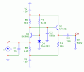
Yes, as I already have said, and the first transistor does exactly the opposite, so I thought the things may get better if you omit both…Elso Kwak said:Current to voltage conversion takes place at the 33 Ohm resistor.
Ok, here is something for which I would say can be made relatively fast starting from the circuit you are using now.Peter K said:Of course I am interested in every improvement, but I need a little help choosing new resistor values etc.
Signal should be tapped in that way the existing I/V resistors stay out of the working circuitry (simplest, disconnect both them and the first transistors). You could leave existing 100pF caps but you can try higher values as well. C1 (1n or something) you could add additionally. R3 should be the trimming pot of 4.7k or 10k and it should be tuned for zero DC at the Q2’s emitter.
I think there is one practically the same circuit (without buffer) posted earlier on this forum as there are numerous suggestions for the improvement (addition of a current sink and a current source for the Q2, current source for the voltage reference (which can be a transistor connected in a few ways), addition of the folded cascode, current mirror). I have not built the circuit as shown below but I guess it can give the idea of how this kind of circuit can perform.
Pedja
Attachments
- Status
- This old topic is closed. If you want to reopen this topic, contact a moderator using the "Report Post" button.
- Home
- Source & Line
- Digital Source
- Noise problem on TDA1541A output