because its a flawed idea...
'so called' high end, elevating 'your original idea' above the high end, before you have even made it work? 512x 384khz? really, are you sure you are half way through this design? if so, are you really surprised that it didnt work? think about that for a minute...
Hard work, inspiration and innovation is what is needed for something hi-end (at least in my definition), not just overkill datasheet perversion. you highlighted via L as a jitter buggaboo, but replaced it with significant added trace inductance. the clock traces dont look 22-33Ω (did you calculate this? how much L for the via and how much L for your alternative?). the i2s output is unterminated and the pads you are supposed to cut (an act that will create unpredictable and inconsistent lumped elements) will look like a parasitic inductor + capacitor + dipole antenna at 200MHz.
a µvia (or a few in parallel) in pad in a 4 layer board is really not going to cause more jitter than a long trace to avoid it and is a whole lot more predictable. Given the jitter is in the ns range on all but mck, is that really worth focusing on?
MBL, Pioneer/TAD, Accuphase, Naim all did something with multiple uber dollar clocks. not for every single sample rate, why? thats what you need to ask yourself. i'd love to see the clean layout, ultra-low noise PSU, reclocking/buffering/MUX system for 8 clocks good enough to generate an advantage. the best ideas are often simple solutions.
using the lowest FS possible gives the lowest noise, why would you want it to be 512x FS? so its close to the 500khz? no reason to use 512x, use 256, any speed that the dac will see will go into 256x FS XO just as cleanly, more cleanly in fact, with lower noise; and it will actually work for 352.8/384khz
512 x 384khz is 196,608MHz, almost double the MAX clock speed SOA. Where will you find a custom low jitter 196,608MHz XO that somehow brings better performance than low jitter 90/98 that are already not easy to find.
are you sure you really did anything with this idea?
but thats enough fro me here, really and i'm sure thats welcomed; at least until some real objective information is proffered.
Hater gotta hate.
Diyinhk - you can send I2S lines straight so I2S socket is left side, not center ? Maybe make no different but keep hater shut up so everybody happy.
")
because its a flawed idea...
'so called' high end, elevating 'your original idea' above the high end, before you have even made it work? 512x 384khz? really, are you sure you are half way through this design? if so, are you really surprised that it didnt work? think about that for a minute...
Hard work, inspiration and innovation is what is needed for something hi-end (at least in my definition), not just overkill datasheet perversion. you highlighted via L as a jitter buggaboo, but replaced it with significant added trace inductance. the clock traces dont look 22-33Ω (did you calculate this? how much L for the via and how much L for your alternative?). the i2s output is unterminated and the pads you are supposed to cut (an act that will create unpredictable and inconsistent lumped elements) will look like a parasitic inductor + capacitor + dipole antenna at 200MHz.
a µvia (or a few in parallel) in pad in a 4 layer board is really not going to cause more jitter than a long trace to avoid it and is a whole lot more predictable. Given the jitter is in the ns range on all but mck, is that really worth focusing on?
MBL, Pioneer/TAD, Accuphase, Naim all did something with multiple uber dollar clocks. not for every single sample rate, why? thats what you need to ask yourself. i'd love to see the clean layout, ultra-low noise PSU, reclocking/buffering/MUX system for 8 clocks good enough to generate an advantage. the best ideas are often simple solutions.
using the lowest FS possible gives the lowest noise, why would you want it to be 512x FS? so its close to the 500khz? no reason to use 512x, use 256, any speed that the dac will see will go into 256x FS XO just as cleanly, more cleanly in fact, with lower noise; and it will actually work for 352.8/384khz
512 x 384khz is 196,608MHz, almost double the MAX clock speed SOA. Where will you find a custom low jitter 196,608MHz XO that somehow brings better performance than low jitter 90/98 that are already not easy to find.
are you sure you really did anything with this idea?
but thats enough fro me here, really and i'm sure thats welcomed; at least until some real objective information is proffered.
This is a module for diyer to enjoy, there are limitless possibility.
Everybody are welcome to mod it with their revolution idea and share the modification experience to the others!
There should be no competing board behind, it should be the first i2s board using the new xmos with 48Mhz oscillator and support 384khz. my competition is always to myself
µvia resistance is very high and it is not good for great decoupling, the pcb bottom layer is already a solid ground plane, there is no advantage to make it 4/6/8/10 layer except for marketing to novice. btw1000k=1M
The datasheet of XMOS has detail specification including the basic pin io clock maximum value. the generous XMOS web site also has many good article from the basic.
Can we only limited to technical exchange and mod on this board rather than ruin the thread with unrelated content?
Last edited:
believer's gotta believe.. halleluiah!!
the trace thing was just a minor detail to illustrate a pattern of ticking buzzword checkboxes and telling a story beforehand, in place of doing the work and varifying the result. here we have talk of a module with over $250 just in clocks and the story of its pure high end beating greatness is fundamentally flawed
the trace thing was just a minor detail to illustrate a pattern of ticking buzzword checkboxes and telling a story beforehand, in place of doing the work and varifying the result. here we have talk of a module with over $250 just in clocks and the story of its pure high end beating greatness is fundamentally flawed
22.5792 and 24.576 is not suitable for ES9018 384khz (synchronous) with the oversampling filter on, you need to run sync mode using the clocks on the module with the OSF off, or run asyn mode and dont use the clocks on the xmos board.
figured you would know that... those speeds are only suited to 88.2/96khz if you want the oversampling filter on. which means you would have to have an MCU to set those registers, like arduino or equivalent. OSF is on by default
Again, please re-read what I actually wrote (ignoring the obvious typo in 22.5792..)
rsowen said:Yes you are going to want a 22.5892MHz and 24.576MHz oscillators ideally. You can use other multiples, but most designs generally use these.
In the general-case, 64Fs * 384 = 24.567MHz. You can use other multiples.
By the way, the XMOS software by default is actually not supplied with 384 support - it has been added by the module provider. (The definition of "most designs" may not even include 384kHz support, but it's all relative I suppose)
I will be adding 384kHz support to the default reference software release in the near future, this is mainly to reduce the support burden of supporting others doing it. I have some DSD functionality and customer projects to finish off first though.
Btw if you are not using the async rate converter mode you won't be worried about BCLK jitter then.
Regarding the setting of configuration registers, I would use the XMOS device to set these, but this is quite hard for a generic module.
Last edited:
simply the constant 512x FS thing
352.8kHz x 512 = 180.6336Mhz
384kHz x 512 = 196.608Mhz.
which clocks at this speed will be used?
what dac will accept them?
256 will work with ESS, but not much else. according to a single person the ESS can be overclocked this much with the OSF turned off, but its double the MAX recommended and nobody else has ever seen it done in reality, it starts getting glitchy @120-140MHz before falling silent and other dacs will have died long ago
This is a module for diyer to enjoy, there are limitless possibility.
Everybody are welcome to mod it with their revolution idea and share the modification experience to the others!
There should be no competing board behind, it should be the first i2s board using the new xmos with 48Mhz oscillator and support 384khz. my competition is always to myself
µvia resistance is very high and it is not good for great decoupling, the pcb bottom layer is already a solid ground plane, there is no advantage to make it 4/6/8/10 layer except for marketing to novice. btw1000k=1M
The datasheet of XMOS has detail specification including the basic pin io clock maximum value. the generous XMOS web site also has many good article from the basic.
Good luck with it I say
You mention modding, is your vision hardware mods only or software also? If the latter, I see the module has a flash on board, is this security protected at all, or are you expecting people to play with the software also? Can we only limited to technical exchange and mod on this board rather than ruin the thread with unrelated content?
I agree.
Again, please re-read what I actually wrote (ignoring the obvious typo in 22.5792..)
In the general-case, 64Fs * 384 = 24.567MHz. You can use other multiples.
By the way, the XMOS software by default is actually not supplied with 384 support - it has been added by the module provider. (The definition of "most designs" may not even include 384kHz support, but it's all relative I suppose)
I will be adding 384kHz support to the default reference software release in the near future, this is mainly do reduce the support burden of supporting others do it. I have some DSD functionality and customer projects to finish off first though.
Btw if you are not using the async rate converter mode you won't be worried about BCLK jitter then.
Regarding the setting of configuration registers, I would use the XMOS device to set these, but this is quite hard for a generic module.
how about reading what I wrote?
64x FS is only in spec with ESS if the oversampling filter is disabled. with oversampling enabled, with the clock speeds you mention, only 88.2/96khz are running in spec. normally 256x FS is used with the oversampling enabled, but the datasheet states a minimum of 192x.no argument with the rest, well just one, bclk jitter is still there if you arent running async, it just doesnt cause dropouts, or force a more relaxed DPLL setting. in fact the PLL is still enabled, the DPLL is just not having to do anything when the clocks are aligned, but the jitter is still there and has to be dealt with.
honestly if you had just put some basic reclocking on there at the output of the reference design and made users more aware of the issue I wouldnt have said anything, because its really not a huge deal to fix and would never effect anything I used it with, so its not a dealbreaker. All my dacs are reclocking dacs, but it shouldnt be there and as a result its present on any of the designs that dont reclock, because they dont know its important unless they measure, people dont always measure...
The secondary point was as important or perhaps moreso, some dacs have issues with jitter on BCK (not just old ones, but yes dominated by older ones, which do still feature heavily enough in todays products and the stuff people use in their homes, to not be ignored) . Some use it as the primary clock.
I know ESS is starting to seem like the only dac out there and I sure favor it, but we shouldnt start acting as f it IS the only dac out there.
Last edited:
unrelated? you brought it up diyinhk, you brought it up as something amazing, the next progression of this design that includes never before heard 8 clocks running at an amazing and consistent 512x FS.
how about sticking to stuff you have verified, rather than making up psuedo-technical bullet points? if you hadnt noticed those are the only things ive picked on. I know its the audiophile way and its tempting to differentiate your design with them, but how about actually differentiating your design instead of marketing primarily on price? you can still keep in theme with the application note recommendations and have some fun. for example a really great power supply for the clock, good common mode and differential filtering etc. onboard isolation, well executed termination etc.
you missed the point about the 4 layers too, because the vias are shorter with 4 layers, they dont have as much inductance as 2 layers and placing a few in parallel, in the pad itself, also lowers the inductance
Last edited:
the trace thing was just a minor detail
Yes. But you want argument for this. Why ? Argument make you happy.
Before you promise you not write until data is on. But you write because argument make you happy.
You argue with main XMOS engineer ! It is not for design of IC. It is because argument make you happy.
I think you have real problem. Maybe you have little bit Asperger Syndrome ? If yes, I am sorry and I hope you find help.
I ask moderator to stop you because I think you cannot stop. Sorry.
how about reading what I wrote?
Precisely. I would suggest your example is not "most designs", but as I said it is relative. For me ESS based systems probably make up around <2% of what XMOS is involved with, for you maybe it is nearer 100%. You example is then also based on a certain mode of this DAC.... I know ESS is starting to seem like the only dac out there and I sure favor it, but we shouldnt start acting as f it IS the only dac out there.
Regarding the bclk jitter stuff, obviously the the clock that the DAC is using for rendering the audio is highly important no one is going to argue this - designs should account for this. Everything else doesn't matter, its just about data-transfer. I've had this conversation with some DAC product designers previously a couple of years ago, a DAC IC designer was on copy. The thread didn't last too long.
If you want to re-clock everything go right-ahead (lets hope you don't hit any metastability issues). I even know some designers that do it for "show" rather than functionality, since they know it will be measured in this community.
Qusp, please do not feel offended if I do not reply to any other comments on this, I'm afraid I've been through this loop a few times before. As I said, I signed up to help people with their DIY projects, not discuss points like these.
Last edited:
haha youre funny, you quote me directly and provoke me with smart *** or clueless comments and then complain when I reply?
whos the one with issues? you are the one throwing the personal characterizations around and you report me? I repeat, this is a technical forum and all people and manufacturers alike should expect to back up their claims or at least not get stroppy when asked to
actually I would say that my conversation with rsowen has morphed more into discourse than argument.
its fine if you are willing to just accept the made up marketing thats handed to you, I dont and I dont think it has a place here in open forum
Yes. But you want argument for this. Why ? Argument make you happy.
Before you promise you not write until data is on. But you write because argument make you happy.
You argue with main XMOS engineer ! It is not for design of IC. It is because argument make you happy.
I think you have real problem. Maybe you have little bit Asperger Syndrome ? If yes, I am sorry and I hope you find help.
I ask moderator to stop you because I think you cannot stop. Sorry.
Last edited:
rsowen, i'm going to take this to PM with you, I had a reply mostly written out but the strange cheerleader distracted me, if i'm going to write it again it may as well be PM.
dont worry I wont carry it on, I have some genuine, somewhat offtopic for this thread questions for you. I feel youve also been caught up somewhat in issues that are not your concern mixed in with some real concerns that I have with the product (multichannel). Now that the somewhat reddish/pinkish mist has cleared a bit on both sides it may be better to do it privately, not being a commercial thread...
dont worry I wont carry it on, I have some genuine, somewhat offtopic for this thread questions for you. I feel youve also been caught up somewhat in issues that are not your concern mixed in with some real concerns that I have with the product (multichannel). Now that the somewhat reddish/pinkish mist has cleared a bit on both sides it may be better to do it privately, not being a commercial thread...
Last edited:
Disagree.µvia resistance is very high and it is not good for great decoupling, the pcb bottom layer is already a solid ground plane, there is no advantage to make it 4/6/8/10 layer except for marketing to novice. btw1000k=1M
microvia resistance negligable and for decoupling is imaterial, it is inductance that is the concern (approx 0.0004 Ohms).
4 layers would allow for interplane capacitance on the power pair, improving decoupling, this would improve the decoupling further and would allow more room to optimise routing. Also it would improve the impedance of the power supply to the pins of the device and the decoupling caps.
This would also allow for a decent ground plane directly under the top layer optimising signal transmission. For the difference in cost you would get a much better product, and more in keeping with a higher end audio image.
Microvias would be a bit of overkill for this design, but personaly I would feal better parting with my money if it was a 4 layer design. Even nicer but costly would be a HDI design with outer layers all ground and signal burried on the first layer down.
All that said the simplicity of the design allows it to be done on two layers and work, the above points I made are just going the liitle bit extra for the best signal integrity.
diyinhk,
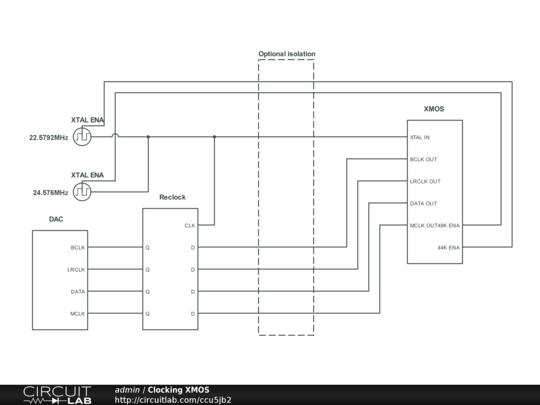
Is there a possibility to use external 22.5792/24.576MHz oscillators from other board, control them by XMOS, and feed their output to XMOS IC?
So
- USB will be asynchronous
- All the jitter will depend on the oscillators used, only them and nothing else.
- This way you can minimize the XMOS bypass/regulators price e.t.c., as long as it will work without issues - no need to have clean supplies, jow-jitter clocks etc on the board.
Then any DIYer would buy the crystek oscillators, connect their OUT pins together and feed them into XMOS and reclock on the DAC side, connect the ENABLE pins to the XMOS so XMOS will switch between 22.5792/24.576MHz clocks.
This way you both get cheap PCB of XMOS, lowish jitter of crystek and, if you want, you can throw some isolation ICs between DAC+Clocks and XMOS.
Absolutly-perfect-solution.
This way:
Last edited:
diyinhk,
Is there a possibility to use external 22.5792/24.576MHz oscillators from other board, control them by XMOS, and feed their output to XMOS IC?
So
- USB will be asynchronous
- All the jitter will depend on the oscillators used, only them and nothing else.
- This way you can minimize the XMOS bypass/regulators price e.t.c., as long as it will work without issues - no need to have clean supplies, jow-jitter clocks etc on the board.
Then any DIYer would buy the crystek oscillators, connect their OUT pins together and feed them into XMOS and reclock on the DAC side, connect the ENABLE pins to the XMOS so XMOS will switch between 22.5792/24.576MHz clocks.
This way you both get cheap PCB of XMOS, lowish jitter of crystek and, if you want, you can throw some isolation ICs between DAC+Clocks and XMOS.
Absolutly-perfect-solution.
This way:
OF course having clean supplies and a low jitter clock on board next to the XMOS as the design has is the best option, it is keeping the clock tracing short, putting a clock through wires and connectors is not the best solution.
s2tup, the idea seems reasonable to me. Unlike a DAC IC, the XMOS chip doesn't care about the quality of the MCLK provided to it - it's just counting MCLK ticks to use as feedback to the USB host to maintain its buffers correctly. The module would need to provide a clock-select line or similar as you suggest. The user would then be free to provide their own clocking etc.
Actually, this is exactly how our latest reference board is setup. All the digital stuff is on a "Core" board with all the audio stuff on a separate board connected via a PCI-E edge connector. Our intention with this system is that we can easy prototype different audio boards and other application interfaces (ethernet, serial, LCDs, etc) without having to touch the "core" stuff every time.
So the clock on a DAC board fed back to the XMOS?
Sure, sounds like reasonable doesn't it? The quality of the MCLK at the DAC is important but not at the XCore. Problem is, the "audio" dongle becomes more of a, um, well a "dongle" I suppose!
... As I said, I signed up to help people with their DIY projects, not discuss points like these.
Appreciate you spending time in this board.
diyinhk,
Is there a possibility to use external 22.5792/24.576MHz oscillators from other board, control them by XMOS, and feed their output to XMOS IC?
So
- USB will be asynchronous
- All the jitter will depend on the oscillators used, only them and nothing else.
- This way you can minimize the XMOS bypass/regulators price e.t.c., as long as it will work without issues - no need to have clean supplies, jow-jitter clocks etc on the board.
Then any DIYer would buy the crystek oscillators, connect their OUT pins together and feed them into XMOS and reclock on the DAC side, connect the ENABLE pins to the XMOS so XMOS will switch between 22.5792/24.576MHz clocks.
...
I can't see under the xmos chip, but if you look closely, it seems it is already configured this way. The enable line are coming from under the XMOS. You could easily test it by measuring the enable pin while switching sample rates. Then just remove the local clocks and feed your clocks.
- Status
- Not open for further replies.
- Home
- Source & Line
- Digital Source
- New XMOS usb 384khz