Hi Tom,
glad to see that they improve their data sheets.
If 10V/ns are sufficient or not, may depend on the specific application.
In my current design it would not be sufficient.
First I was checking if the IRFB4615 would work for me.
It is a pretty nice and fast switch, but with limited power handling capabilities.
Found that its limitations are in the range of 25-30A, when hard switching with 400kHz.
So I am right now planning to use the IRFB4115, of course they need a stronger gate drive compared vs 4615...
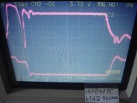
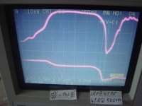
Attached two screen shots when operating the IRFB4115 at 41A continuous current load under hard switching conditions with 500kHz (I usually simulate heavy bass load by loading the half bridge with constant current. Simply a series of some hundrets mOhms + 20uH from half bridge output to positive rail and duty cycle adjusted to get the desired current).
The first step in Uds is caused by the massive di/dt during commutation from upper Mos to lower Mos. This di/dt is above 1000 A/us and causes an inductive drop around 30V. Please note the RdsON and the dead time are chosen in a way that the body diodes do not store much charge. So I do not need to remove full Qrr.")
After 41,6ns the current has commutated to the lower switch and the half bridge output jumps within 4ns to the lower rail. The resulting dv/dt is around 15V/ns.
Upper Trace: Ugs of lower Mos, 5V/div
Lower Trace: Uds of lower Mos, 50V/div
glad to see that they improve their data sheets.
If 10V/ns are sufficient or not, may depend on the specific application.
In my current design it would not be sufficient.
First I was checking if the IRFB4615 would work for me.
It is a pretty nice and fast switch, but with limited power handling capabilities.
Found that its limitations are in the range of 25-30A, when hard switching with 400kHz.
So I am right now planning to use the IRFB4115, of course they need a stronger gate drive compared vs 4615...
Attached two screen shots when operating the IRFB4115 at 41A continuous current load under hard switching conditions with 500kHz (I usually simulate heavy bass load by loading the half bridge with constant current. Simply a series of some hundrets mOhms + 20uH from half bridge output to positive rail and duty cycle adjusted to get the desired current).
The first step in Uds is caused by the massive di/dt during commutation from upper Mos to lower Mos. This di/dt is above 1000 A/us and causes an inductive drop around 30V. Please note the RdsON and the dead time are chosen in a way that the body diodes do not store much charge. So I do not need to remove full Qrr.
After 41,6ns the current has commutated to the lower switch and the half bridge output jumps within 4ns to the lower rail. The resulting dv/dt is around 15V/ns.
Upper Trace: Ugs of lower Mos, 5V/div
Lower Trace: Uds of lower Mos, 50V/div
Attachments
The 41.6ns is the time for both.
Taking over the load current and removing Qrr.
First the current in the lower switch rampes up to full load current,
then continuos to ramp up further to remove the Qrr.
Already with Qrr=0, we would need a di/dt around 1000A/us to commutate 40A within 40ns.
If you increase the dead time, then the current will commutate to the body diode right after turning OFF the upper switch but before the lower switch turns ON.
If you avoid long dead times, then the process of becoming non conductive of the upper switch and becoming conductive of the lower switch happen in parallel. The diodes will see just very few charge. The amount of charge which we have to remove is not larger than the amount of charge that was applied during forward time of the diodes.
You need high switching precision for such an adjustment, but it is possible.
If you introduce longer dead time in the above set up, then the time for commutation will increase significantly and the losses too.
Drawback of the chosen dead time setting is that the adjustment, which is perfect at high load, will cause a significant cross conduction peak during idle condition. Overall it is a trade off, which everybody has to settle in his design, according his requirements.
If you optimize for low idle losses, your switches will struggle more with Qrr at high loads....
High dv/dt will happen in any case, the more Qrr you have to remove the more tough. ..oh yes the diode snap off right after Qrr is removed is no fun.
Snubbers could theoretically help to reduce dv/dt even further.
But consider which values you will need.
Let's assume the body diode might have not been fully flooded.
May be the Qrr removing current was just 20A (which are on top of the 40A), then the lower Mosfet will be in the situation of drawing 60A in the moment of diode snap off. 40A will be delivered by the load, the other 20A will have to be catched by the snubbers and parasitic capacitances.
The shown screen shot was taken with 470pF+12 Ohms directly from drain to source at each switch.
I forgot to highlight one other effect.
The massive dip in Ugs in the moment of sloping.
Most people think it would be caused by the Miller capacitance.
In fact that's just one portion of the dip.
The larger portion is caused by the huge 'snap off di/dt' of the diode.
The upper body diode snaps off and suddenly the lower Mos does not need to carry the removal current anymore. Means the current in the switch has to come down from i.e. 60A to 40A very fast. Lead inductance of the TO-220 source lead will show a significant voltage drop, which we see as a dip when measuring the Ugs.
Excellent work with di/dt!!
Waveforms look quite good. Turn off would be even better with slightly lower gate drive inductance. The glitches in gate drive (due to buffers?) could be smoothed out too.
470pf + 12 ohms seems a bit "light", and ringing looks slightly underdamped. What is the frequency of the major resonant mode that appears without snubber? I get over 100Mhz with IRFB4227 (lower Cds). Did you try to tune C and R parasitic inductance at the main mode and then reduce R until best damping is achieved? A good start value is a C similar or slightly higher than Cds at max. typ turned-off Vds.
Guess what? I have just confirmed that my big sub amps with "crazy switching" pass radiated EN55022B, two dominant peaks appear in the spectrum. One is associated with turn on slopes and the other associated with turn off slopes (its harmonics are slightly noticeable too). A smaller and lower Q peak appears around FET resonant mode too. Small ferrite bead was needed in speaker wires in the end (ceramic chips to case/gnd not practical in this design).
Waveforms look quite good. Turn off would be even better with slightly lower gate drive inductance. The glitches in gate drive (due to buffers?) could be smoothed out too.
470pf + 12 ohms seems a bit "light", and ringing looks slightly underdamped. What is the frequency of the major resonant mode that appears without snubber? I get over 100Mhz with IRFB4227 (lower Cds). Did you try to tune C and R parasitic inductance at the main mode and then reduce R until best damping is achieved? A good start value is a C similar or slightly higher than Cds at max. typ turned-off Vds.
Guess what? I have just confirmed that my big sub amps with "crazy switching"
pass radiated EN55022B, two dominant peaks appear in the spectrum. One is associated with turn on slopes and the other associated with turn off slopes (its harmonics are slightly noticeable too). A smaller and lower Q peak appears around FET resonant mode too. Small ferrite bead was needed in speaker wires in the end (ceramic chips to case/gnd not practical in this design).
Last edited:
Hi Eva,
my congrats that you passed radiated EMI
Dominant resonant mode without snubbers in this bread board up was below 100MHz. Would need to measure again, but I think it was around 80MHz.
Based on your older hints and findings of my older proto (4 years ago), I also experimented with the geometry of the snubbers, but strangely - this time it showed just a minor effect in this bread board.
470pF are light? Hm, 2 years ago I tweaked my old proto to 1MHz switching frequency and reduced the snubber caps for the IRFB4321, because of heat. There I found a cool snubber geometrie which was perfect with 220pF and approx 10 Ohms. Well, cool from damping effect, but the necessary snubber loop was in the category of 10cm² ! ...having some doubts that this would be fortunate for radiated EMI.
Lower gate resistor for turning OFF:
It seems that I am already touching the limitations of the parasitic inductance of my gate drive loop in that proto.
Glitches:
The glitches at the end of turning OFF seem to be related to the reverse recovery of the boot strap supply diode. Originally it was much larger. Changing the charge pump wiring and also optimizing the boot strap diode reduced the glitches to a reasonable level.
...let's see how things will come with a proper PCB.
This time I am definitely on the trip to settle a nice amp with double layer PCB, in order to play around with a new gain and loop topology that overcomes a good portion of the distortions, which are related to the carrier residuals in clocked post filter designs. In simulation it appears great, time to go for the real thing. Playing with KiCad these days...
Tom:
Sorry for 'off topicking' your thread.
my congrats that you passed radiated EMI
Dominant resonant mode without snubbers in this bread board up was below 100MHz. Would need to measure again, but I think it was around 80MHz.
Based on your older hints and findings of my older proto (4 years ago), I also experimented with the geometry of the snubbers, but strangely - this time it showed just a minor effect in this bread board.
470pF are light? Hm, 2 years ago I tweaked my old proto to 1MHz switching frequency and reduced the snubber caps for the IRFB4321, because of heat. There I found a cool snubber geometrie which was perfect with 220pF and approx 10 Ohms. Well, cool from damping effect, but the necessary snubber loop was in the category of 10cm² ! ...having some doubts that this would be fortunate for radiated EMI.
Lower gate resistor for turning OFF:
It seems that I am already touching the limitations of the parasitic inductance of my gate drive loop in that proto.
Glitches:
The glitches at the end of turning OFF seem to be related to the reverse recovery of the boot strap supply diode. Originally it was much larger. Changing the charge pump wiring and also optimizing the boot strap diode reduced the glitches to a reasonable level.
...let's see how things will come with a proper PCB.
This time I am definitely on the trip to settle a nice amp with double layer PCB, in order to play around with a new gain and loop topology that overcomes a good portion of the distortions, which are related to the carrier residuals in clocked post filter designs. In simulation it appears great, time to go for the real thing. Playing with KiCad these days...
Tom:
Sorry for 'off topicking'
your thread.Diode forward and reverse recovery processes are symmetrical. The charge that takes 100ns to be removed from the diode took another 100ns to be stored... Oh, wait, was the diode allowed to conduct full output current for so long? Obviously no.
Obviously not.
In fact, it can be worse than that. Far worse.
When a diode is forward-biased at high dI/dt, it can develop a forward voltage of 20, 40, even 100 volts at very high rates -- and this is a real voltage applied to the junction, it is not due to lead inductance, which does increase the apparent measurement, but does not account for the whole thing. Quite simply, the instant you apply voltage, there's no charge in the diode (assuming it's initially off), so the voltage can be pretty much anything until charge carriers flood across the junction and it becomes conductive.
When forward-biased suddenly, charge drifts into the junction, and it gradually becomes more conductive. If you reverse-bias it within the transit time, you can generate clouds of charge within the junction. Even if you simply reverse-bias a quiescent (fully saturated, steady state, whatever) junction, you can get behavior where regions of the junction deplete sooner than others.
When packets of charge occur, the junction is effectively shorted out in part. If the other part comes out of recovery, it becomes an insulator. Now the full reverse voltage appears across a narrow thickness of the junction, and the avalanche voltage is effectively reduced -- this can lead to a phenomenon known as dynamic avalanche, where it might break down (causing excessive losses and ringing) at a fraction of the rated voltage. This is particularly important under conditions of high voltage, high dI/dt and large stray inductance, which are precisely the conditions you'll get under arbitrary load current, short deadtime conditions.
Now, power diodes don't usually have the same doping profiles as SRDs (step-recovery diodes), but under the right conditions they can behave in exactly the same way. This can lead to incredibly high dV/dt recovery slopes, resulting in excessive EMI and potentially dangerous peak voltages. The trigger is usually short on-times and high dI/dt recovery conditions.
The biggest issue is high voltage diodes, where the junction width is necessarily large. This is a concern to myself, because I regularly work with 480VAC input circuitry, which typically requires 1200V rated diodes, which have wide junctions, giving ample time for transition time effects to take effect.
On the plus side, 200V diodes are substantially faster (and there are silicon schottkies available, completely obviating this operating condition), which makes class D operation easier. Still, it won't completely go away; forward and reverse peak voltages are always a concern, and small changes can cause large EMI problems. The best solution is to always be aware of these limits and design accordingly. You can usually do better by reducing stray inductance and capacitance, but increased stray inductance and snubber capacitance often improve switching, rather than impairing it as many believe.
Tim
Sch3mat1c: You are extrapolating data from another type of semiconductors and circuits.
The substantial forward voltage spike already seen on 600V ultrafast diodes when starting conduction is almost gone in body diodes of low voltage MOSFET. Old IR datasheets just said "intrinsic body diode turn on time is negligible" instead of giving a forward recovery time rating.
The IR series of MOSFET we talk about have a Vds rating of 250V or less, and are intended for synchronous rectification among other things. The dies are designed to get both low Rds-on and a decent ultrafast diode, and the cell structure of the MOSFET (like many transistors in parallel sharing a PTC resistive common collector connection) stores more than an order of magnitude less charge than the devices you are used to. Only a too high di/dt and dv/dt and Id combination can make the diode fail, and the failure mode is latching due to parasitic thyristor, not "hot spot" style failure.
In fact, maximum practical MOSFET (forward) turn-off di/dt is not much higher than the recovery di/dt allowed by the diode, 2:1 or less. Industrial switching in my opinion will take years to reach that degree of refinement.
Last edited:
Concerning turn off, I meant reducing loop inductance, not the resistance.
Yup, thinking the same.
With "light" I meant too high resistance, capacitance is probably ok.
Just looked to the bread board again. It is a parallel connection of 5x
47 Ohms. Ok, it's not 12 Ohms, but 9.4 Ohms. ...for some reason I had in mind that I found the optimum around 12 Ohms.
Anyway, I will have to readjust the snubbers according the PCB in any case.
Worth reading:
http://www.google.com/url?sa=t&rct=...sg=AFQjCNH_iX78PGHJIcczAxGZ8SH-j2k2NA&cad=rja
I am still convinced that the body diode in my case is acting more or less in soft recovery and the first step in Uds is really an inductive phenomenon.
Coming from a di/dt of slightly above 1000A/us, this 30V step would correspond with loop inductance of less 30nH. These 30nH would reflect the source lead inductance of the upper Mosfet + drain lead inductance of upper MosFet + inductance of upper ceramic cap + inductance of lower ceramic cap + inductance of board connections.
I doubt that this sum is much less than 20nH-30nH and consequently Kirchhoff leaves not much space for a high voltage peak across the junction in my set up.
Up to now I did not manage to kill the IRFB4115. Also all measured values are within allowed limits of the data sheet.
But previously I examined limitations of IRFB4615 at 400kHz and +/-60V.
First I operated with moderate di/dt and got failures already short above 20A load current.
The higher I adjusted di/dt the higher the limits moved and I could shift the failure limit to approx 30A.
I think in case of IRFB4615 I always had the body diode flooded, before
turning ON the other switch- just because of the high Rdson, which cannot bypass very high currents from the diode.
To me all findings indicate that we can assume soft recovery of the body diodes in these types under all conditions, that I tested.
Well - even 'soft recovery' still involves giant di/dt at the end of reverse recovery that triggers resonances of the circuit, if not snubbered properly.
Aren't your ceramic capacitors from positive rail (upper source) to negative rail (lower drain)? This may result in a slight improvement in inductance (if mated with layout).
Usually I am placing both MosFets side aside, in this case the distance from upper drain to lower source is given by the MosFet geometry and is longer than two SMD caps anyway. I am using multiple parallel strings of two series caps. Center tap has a less relevant connection to GND.
In fact in this particular set up I placed both MosFets with a certain distance inbetween, because I also experimented with the old source inductance di/dt limiter. For these MosFets I came to the conclusion - the faster the better.
Final gate drive wiring was connected directly to the MosFet legs and
connections of the power loop with flat copper plates.
Final PCB will have the MosFets close together....
Final gate drive wiring was connected directly to the MosFet legs and
connections of the power loop with flat copper plates.
Final PCB will have the MosFets close together....
Anyway, I will have to readjust the snubbers according the PCB in any case.
What should one generally be looking for on Vds waveforms in order to properly optimize these snubbers?
This one looks promising
http://ixapps.ixys.com/DataSheet/DS99220F(IXFH-FT-69N30P).pdf
300V, 69A, Trr=100ns, Qrm=500nC, Rds=0.049ohm
http://ixapps.ixys.com/DataSheet/DS99220F(IXFH-FT-69N30P).pdf
300V, 69A, Trr=100ns, Qrm=500nC, Rds=0.049ohm
- Status
- This old topic is closed. If you want to reopen this topic, contact a moderator using the "Report Post" button.
- Home
- Amplifiers
- Class D
- new MosFETs on the block...