Hello
Hey Pred velcome back->glad to hear et went well
Now to work
Hey Pred velcome back->glad to hear et went well
Now to work
TL431:
I would put always the capacitor over the "higher" resistor in the TL431 power supplies (R3 and R20 in the receiver schematics). It makes a unity gain circuit at higher frequencies and has a lower noise (look at TNT measurements). Since the circuit works properly it can be left out (some people think that this circuit "sounds" better without but engineer in me would put it). Do we really need 3 capacitors since the circuit will be so close to the chip? As I sad a succesfull project is full of compomises and you can leave them since I do not have to install them.I think it´s a good idea to bypass the top resistor in each shuntleg->It´just don´t make a big different when you have such low values (330R and 1K)
But what capacitor value anyway 1->10uF??
I have chosen three capacitors to get a good damping off high frequency noise. (others use 1nF instead off the 10nF)
please comment here if you got a suggestion
I thought we would use OSCONS for C15 and C7 in the same schematics?Yes all are oscons SP series exept the 220uF in 5V dac analog supply
I would set BG there because off soundquality
Do OSCONS exist as SMD? Finally sinking 50mA through TL is an overkill IMHO. Minimum 2mA is needed so 10 including the 1k 330Ohm divider should be enough. Since we are going to use CCS for feeding (it is wired which I like ) the DAC I think they should be on the power supply separate PCB. In that sence has someone knows a good way for wiring the PCBs together at least for PS? I always used soldering but when you try to change somethinh it becomes a pain. Recently did tube preamp and had some hum problems. As a "good boy scout" I have made all connections very short. Imagine the problem of turning the PCB soldered on both sides with wires
Why do you want Oscon capacitors in smd?
I think we should use a high as possible current through the TL431 got a low impedance and good dymanic (I think about 10mA to 20mA will work great
I have tested home with a ccs->65mA->Tl431-< will try tonight with 10mA-< sinewave generator->10Hz and up to see how good the tl431 are to suppress noise (outputimpedance)
CS8416:
I like it exept choosing inputs. I would like to have three inputs. If I have time I'd add an USB input. I saw on some shematics that people are using the logical buffer between switch and the circuit. I do not know if it is necessary, does somebody knows? I see you have a button for the reset. I am not sure, but like through the fog, I remember that this chip should be reseted after power up. If so I propose we make a simple NE555 reset circuit using monostable multivibrator.
I don´t know if a 555 reset circuit is nessacary?
You can put it into the circuits if it is
I have used a capasitor and a 4K7 resistor to make "reset time"
Don´t know if the switch is needed?
PCMs:
I would leave the configuration pins to the switches. When I do test ASIC PCBs I make what we call "solder switches". It is like a 0805 SMD support. Just the distance is smaller, in fact a little bigger than the minimum distance between the metalic lines of the PCB process. When you want to connect the two togeter (make a jumper) you just simply solder it down. It cuts costs and it is easy. So you "preview" a default configuration that you think will work and than solder if it is necessary. In this way we could test parallel as well as dual mono configuration. That means you have to leave the outputs not connected together. And since it is a current output it should not be the problem to connect them on the I/v conversion board.
That´s a very good idea tell me more about that
AD1896:
I thought we could go 196k with 27MHz clock? I am not sure about your question and will look into it. We did not discussed any clock solution. Do you plan to leave a place only for Guido's XO on the PCB and someone wants to use another clock should connect it externaly? The same thing for config should be applied here in order to change something if necessary. Any error in configuration that might appear in the design period for mis understanfing of the datasheet could cost us a lot and cutting end changing small lines on these small nasty chip will be pain!
To get 192Khz sampling out off AD1896-> then you have to set it to Slave mode and add a counter and a inverter
This is because AD1896 can only handle a clock off 30Mhz.
Please see the post "AD1896 in slavemode how?"
We can do it if you will make that ekstra components on the Dac pcb
Else I will only put an external clock->because people want to use different clock circuits
Hello
Pred what do you think off the circuit that gmarsch had draw for us , to put AD1896 in slavemode and 192Khz sampling out ?
Remember also that it needs to clocks-> a 27Mhz to set AD1896 maximum working speed
2nd 24.576Mhz clock to feed directly into MCLK at PCM179X
Hve anyone any answer about using a 27.0Mhz clock for AD1896 and PCM1798 in hardwaremode (256FS)???
Best regards
KIm
kimschips said:Hello
Pred what do you think off the circuit that gmarsch had draw for us , to put AD1896 in slavemode and 192Khz sampling out ?
Remember also that it needs to clocks-> a 27Mhz to set AD1896 maximum working speed
2nd 24.576Mhz clock to feed directly into MCLK at PCM179X
Hve anyone any answer about using a 27.0Mhz clock for AD1896 and PCM1798 in hardwaremode (256FS)???
Best regards
KIm
I do not know what circuit you are talking about. Can you point me where it is? In the mean time, two clocks hmmm not really happy with it. People have a lot of problems with only one. Two of them would be even more problematic. Maybe Guido has better idea about that. I must say I am still on vacation and just following the discussion. From next week I plan to redraw your circuit in protel and see. For me if I go up to 96kHz it is OK... I have to look at the datasheets to tell you more. But I am afraid that you have to wait monday tuesday for that
pred said:
I do not know what circuit you are talking about. Can you point me where it is? In the mean time, two clocks hmmm not really happy with it. People have a lot of problems with only one. Two of them would be even more problematic. Maybe Guido has better idea about that. I must say I am still on vacation and just following the discussion. From next week I plan to redraw your circuit in protel and see. For me if I go up to 96kHz it is OK... I have to look at the datasheets to tell you more. But I am afraid that you have to wait monday tuesday for that
Hello Pred
Here are the link for "AD1896 in slavemode"
http://www.diyaudio.com/forums/showthread.php?s=&threadid=63309&perpage=10&highlight=&pagenumber=1
Look post 3 for explanation and post 10 for the extra circuit, that you connect in parrallel with the outputs off AD1896, to get 192Khz sampling out.
The two clocks can both be XO clock from Tentlabs or Elso kwak at->27.0000Mhz and the other 24.5760Mhz (instead off the 49.1Mhz clock in the gmarsch schematic) (remember to change the counter output)
The new settings for each chip, will then be changed to I2S format and Slavemode for AD1896 and PCM179X
So, if you can put two extra chips on the pcb, then let´s go for 192Khz sampling in slavemode.
If you only will upsample to 96Khz just use a 24.576Mhz clock (instead off the 27.000Mhz) and use the schematic as it is (AD1896 hardwaremode).
The thing is that AD1896 can maximum handle 30Mhz clock, (gmarsch use 29.9Mhz) I just recieved a very nice crystal at 27Mhz so I will get samplingrate at 27.0Mhz/256=105Khz.
But if PCM1798 don´t like the 105Khz samplingrate, then I must build a 24.576Mhz clock, or set the dac up in slavemode.
Pred if you draw a new schematic:
Can you add the great ideas from your last post->
"solder switches". It is like a 0805 SMD support"
Make an extra input for the CS8416-> like mine solution without putting in a contac (and long wires) in the input signal path)
Add the circuit for Slavemode (one counter and a inverter)
Pred take your time no need to hurry
All the best
Kim
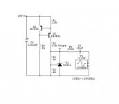
Hello
Here is my little circuit with TL431
The TL431 are from Texas instrument
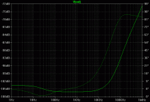
The meausurement is done with a ordinary scope in parrallel with the TL431.
Source:10Vpp signal generator:
10mA-->TL431=8Vpp 10Hz->100Khz
30mA-->Tl431=10mVpp 10Hz->100Khz
As you can see there is a huge different between 10mA or 30mA throught TL431.
A capacitor like a 10uF BG-N is what I got for now-> reduces the impedance above 100Khz so you get a flat impedance from 10Hz to 1Mhz-> at about 0.36R not so low thought
Best regards
Kim
Here is my little circuit with TL431
The TL431 are from Texas instrument
The meausurement is done with a ordinary scope in parrallel with the TL431.
Source:10Vpp signal generator:
10mA-->TL431=8Vpp 10Hz->100Khz
30mA-->Tl431=10mVpp 10Hz->100Khz
As you can see there is a huge different between 10mA or 30mA throught TL431.
A capacitor like a 10uF BG-N is what I got for now-> reduces the impedance above 100Khz so you get a flat impedance from 10Hz to 1Mhz-> at about 0.36R not so low thought
Best regards
Kim
Attachments
kimschips said:Hello
Here is my little circuit with TL431
The TL431 are from Texas instrument
The meausurement is done with a ordinary scope in parrallel with the TL431.
Source:10Vpp signal generator:
10mA-->TL431=8Vpp 10Hz->100Khz
30mA-->Tl431=10mVpp 10Hz->100Khz
As you can see there is a huge different between 10mA or 30mA throught TL431.
A capacitor like a 10uF BG-N is what I got for now-> reduces the impedance above 100Khz so you get a flat impedance from 10Hz to 1Mhz-> at about 0.36R not so low thought
Best regards
Kim
Although I am sick with flu and temperature good thing I have a portable so I can work from bed
. I did some simulations in LT spice with transistor level TL431 model. I think that your circuit is wrong an at least for the test you should put a diode in series with your voltage source. In this case for at least 50Hz you just charge and discharge the capacitor... The best way would be to test your circuit with a dc source and your signal generator on top (maybe a summing circuit with some opamp could come in handy). Thay is how I have simulated using AC simulationsIn my simulations the 10mA current is even better ( I changed R1 from 22R to 55R) -85db of attenuation in a comparison to -76dB. I used different transistors since my model files are at work, but in this case I think that does not change a lot. With capcitor of 22u over R4 things get some dB better. Anyway, I think that there is no big difference and would have to examine the circuit more to see where the difference is coming from, but I still think that 30mA for a to92 pacjage is too much. Is your tl431 geting hot with 30mA?
Pred
Sorry. It seem I have misread your sch. You are pumping an AC signal from the right. I do not know I tried this as well and everuthing seem's more or less the same in simulations at least.... And why should you pump the TL431 like this. The back signal from DAC is on high frequency more than a MHz so you will kill it by the ferite bead?
Pred
Pred
again me after this I promise not to write at least not today.
I saw to some extent in transient analysis what you are talking about. It seems at -4V of the your source generator something starts to happen and the circuit moves for 10mA but not for 30mA. To much fever to look in detail, sorry. Try with +-2V if you can and you will see that they are more or less the same. 2V is more than 100 times bigger that waht you will have in a real circuit. And just looking at those transient curves 10mA still looks a little bit better
after this I promise not to write at least not today.I saw to some extent in transient analysis what you are talking about. It seems at -4V of the your source generator something starts to happen and the circuit moves for 10mA but not for 30mA. To much fever to look in detail, sorry. Try with +-2V if you can and you will see that they are more or less the same. 2V is more than 100 times bigger that waht you will have in a real circuit. And just looking at those transient curves 10mA still looks a little bit better
more on ccs
I have done some simulations of the TL with ccs. I used LT Spice and transistor level TL431 model that could be found in the LT yahoo group.
I will devise this comment in several posts since I do not know how to include several images in one.
First I have started with the original circuit posted by Kim.
Attachments
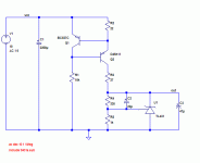
The obtained result of AC simulations for the output give around -85dB of V1 voltage suppresion. The differences were quite small electrically if the current trough the TL were big or small. The problem with Kim's measurement in my opinion is that with high negaitve voltage of his sinus source at the test bench pushed all current trough the output resistor and the TL431 was deprived from the minimum 2mA that it needs to operate properly. In this way he saw a huge difference between 10mA and 30mA of current.
Attachments
improvement on the ccs
Yestrday I was talking to Geoff Moss on a different subject and saw another circuit enhacment that is very easy to implement. Changing the 10k resistor (R1 in my previous post with the) with a constant current diode like j508 (2.4mA).
I did not have any model for a cc diodes so I used a Jfet to simulate the behaviour.
Attachments
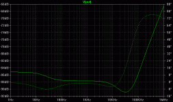
results...
I must add that now we have around 3.5 mA flowing trough the Q1.
In the included image you can see that at least in the simulator the improvement on the PSRR is 20dB. The simulated value is now arround -105dB.
At the same time I have performed a noise simulations and they are more or less the same (nV of difference at 1kHz) for both cases.
Conclusion:
It is a worthwhile mod to try since if we use standard resistor a ccs diode can be soldered in the same place with some bending of the case wires.
What do you think?
Attachments
Hello Pred.
That is very interesting with the jfet in the current source-> looks good .
I think in the real world, you are using a resistor between the Jfet and CCS base-> to set the current.
As you can see the PSRR is very good up to 10Khz
I think it will improve the PSRR, if you put in a Ferrite bead between the 27R resistor and TL431 (as in our schematic)
Finally we can add a LM317 before the CCS to further improve PSRR.
All the CCS (One for each dac chip) will then be connected to one LM317, exept the PCM179X´s will have it´s own LM317)
What do you think about that?
You could also simulate PSRR with C3=22uF in pararalel with a 100nF ceramic (as in our schematic)?
And try without C2 to see the difference.
The CCS current must minimum be 20mA (10mA for TL431 and 10mA for each dacchip PSU. In final CCS current will be 40mA to feed a dacchip (analog and digital).
Kim
That is very interesting with the jfet in the current source-> looks good
.I think in the real world, you are using a resistor between the Jfet and CCS base-> to set the current.
As you can see the PSRR is very good up to 10Khz
I think it will improve the PSRR, if you put in a Ferrite bead between the 27R resistor and TL431 (as in our schematic)
Finally we can add a LM317 before the CCS to further improve PSRR.
All the CCS (One for each dac chip) will then be connected to one LM317, exept the PCM179X´s will have it´s own LM317)
What do you think about that?
You could also simulate PSRR with C3=22uF in pararalel with a 100nF ceramic (as in our schematic)?
And try without C2 to see the difference.
The CCS current must minimum be 20mA (10mA for TL431 and 10mA for each dacchip PSU. In final CCS current will be 40mA to feed a dacchip (analog and digital).
Kim
kimschips said:I think in the real world, you a using a resistor between the Jfet and CCS base-> to set the current.
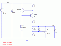
I do not know if we understand each other. Resitor R2 is used to set the current. JFET current source (a diode accualy since I did not have the model) here plays the role to stavilize more the transistor Q1. The principle of this current source is that Vbe of the Q1 is constant no matter how big is the change in current trough the transistor. In most cases this is true but to improve you must stabilize more...
I think it will improve the PSRR, if you put in a Ferrite bead between the 27R resistor and TL431 (as in our schematic)
Ferrite nead has almoust nothing to do with PSRR at least not at low frequencies. It has to do with above 1MHz or so, depending on the resistance and inductance of the bead. The mod that I explained is to improve the low frequency (mostly 50 and 100Hz) suppresion.
Finally we can add a LM317 before the CCS to further improve PSRR. All the CCS (One for each dac chip) will then be connected to one LM317, exept the PCM179X´s will have it´s own LM317)
That is another story and LM317 can be used since it has very good suppresion. I like the serial mosfet regulators (as on tnt convertus) as they have a slow startup. But that is the question of the choice I think as well as you that I would go with LM317. But I think I would devide the digital and analog parts using 2 transformers or at least 2 windings of the same transformer in order to isolate them as much as possible. Also I think we made a great care on the PSU for all components that separate for PCM1798 is an overkill...
You could also simulate PSRR with C3=22uF in pararalel with a 100nF ceramic (as in our schematic)?
Simulating the capacitors is really tricky if you do not know all parameters. LT Spice is nice because you can assign to every capacitor, serial resistance, inductance and other stuff if you know them. For most capacitors they are not even stated in the datasheet. If I put just 100n capacitor it will not change much or it woild improve greatly wich is not the real case. The combination of two capacitors is a trial and error and should be tested in practise.
Pred
Also I think we made a great care on the PSU for all components that separate for PCM1798 is an overkill...
What do you think is overkill for the PCM1798?
We could also here settle with SP Oscons (22uF VCC/VDD and 47uF Vcom)
Then it´s also cheeper when you reduce the numbers off suppliers
A CCS with a Jfet, could be-> put in a resistor between source and ground and then connect the gate to ground
Have you simulated the tl431 without the CCS?
Have you thought about the add on circuit to make upsampling to 192Khz in slavemode?
Kim
kimschips said:What do you think is overkill for the PCM1798?
I thought that you wanted a separate PSU all together for PCMs. Separate LM317 is ok. I thought that maybe I'll use separate LM317 for all local voltages. It depends on the plase on the PCB. The LM317 are very cheap so the cost is not a problem. The size of PCBs that I can produce is 160x100mm so this will be the only limiting factor.
We could also here settle with SP Oscons (22uF VCC/VDD and 47uF Vcom)
Then it´s also cheeper when you reduce the numbers off suppliers
Yes I'll use the OSCONS all around and since it is nothing special to fit any capacitor through two holes it is not big issue in the designing stage
A CCS with a Jfet, could be-> put in a resistor between source and ground and then connect the gate to ground
Yes I know. First this arrangement is only for up to several mA so it cannot be used as a primary CCS that will feed the TLs. Second, the performance of such CCS is almoust order of magnitude poorer than what we use now.
Have you simulated the tl431 without the CCS?
I just did
It has around -60db PSRR. So 20 db less than with current source with resistor or 40 db less than with jfet in place of resistorHave you thought about the add on circuit to make upsampling to 192Khz in slavemode?
Yesterday I've been reading the datasheets both AD1896 and SRC4192. I must admit that for me they are very hard to read so I used the data sheets for the evaluation boards as well. At the end qmarsh was righ AD can not work with single 27MHz clock
. It needs at least 138 times greater clock than 192kHz but then you can not set it for 192kHz. So you need other clock. On the other hand you can use SRC with can do it with single 24.576MHz clock. Sombody sad a lower performance of the SRC to AD but I will check I am not really sure... Did soeone compare.
So there are two solutions:
1. Use SRC with one clock or use AD with 96kHz
2. Use AD with two separate clocks or implement with PLL1705.
PLL1705 can derive all necessary frequencies for AD from a single 27MHz clock. Did someone tested or tried this chip. The datasheet states 50ps of jitter?
Kim: Where is the qmarsh schematic with proposal for two clocks?
I am really busy at work, this seem more complicated than I thought
Pred
pred said:
I just did
Pred
Very good work Pred-> we settle with the oscons and "J508" in the CCS
Yesterday I've been reading the datasheets both AD1896 and SRC4192. I must admit that for me they are very hard to read so I used the data sheets for the evaluation boards as well. At the end qmarsh was righ AD can not work with single 27MHz clock
. It needs at least 138 times greater clock than 192kHz but then you can not set it for 192kHz. So you need other clock. On the other hand you can use SRC with can do it with single 24.576MHz clock. Sombody sad a lower performance of the SRC to AD but I will check I am not really sure... Did soeone compare.
So there are two solutions:
1. Use SRC with one clock or use AD with 96kHz
2. Use AD with two separate clocks or implement with PLL1705.
PLL1705 can derive all necessary frequencies for AD from a single 27MHz clock. Did someone tested or tried this chip. The datasheet states 50ps of jitter?
Kim: Where is the qmarsh schematic with proposal for two clocks?
I am really busy at work, this seem more complicated than I thought
Pred [/B][/QUOTE]
The difference between AD1896 and SRC4196 should be that AD1896 is 600times better than SRC4192 to suppres jitter!
qmarsch schematic can be found here:
http://www.ettnet.se/~tobias/diy/sch.png
qmarch don´t use slavemode, he use hardwaremode (256FS) and upsample to 116Khz sample frequency
But I think we should use 2 clocks
1. 27.0000Mhz and one at 24.576Mhz+ counters and one inverter
I think it´s worth the extra omponents
Please see the post "AD1896 in slavemode"
Kim
kimschips said:
qmarch don�t use slavemode, he use hardwaremode (256FS) and upsample to 116Khz sample frequency
But I think we should use 2 clocks
1. 27.0000Mhz and one at 24.576Mhz+ counters and one inverter
I think it�s worth the extra omponents
Please see the post "AD1896 in slavemode"
Kim
Yes I have found the schematics.
I suppose that both clocks do not have to be good like XO2 since 27MHz is used only for calculation. But I have a problem to find 27MHz clock (DIP8 for possible change with XO).
The other one I have found and it is 20EUR so it is better to order dirrectly from guido... If you want two good clocks you need like 60EUR just for clock's. It starts to go way out of my design plans. I have found some quartz makers here so I will ask for prices or samples if it is possible to obtain.
But still 2 clocks on one board seem like probem to me. I will se if it is possible to create a schematics where the two things could be tried at the same time, just not soldering some of components. I think I would probably go for the 1clock 1src in direct mode. Choosing higher clock you have a higher clocking frequency.
I am quite tired from this troubles about the design in last couple of days. Problem is that we lack experience in this domain and nobody is willing to help. I thought I would make dac board relativly quickly and than have fun with i/v stage.
I will rest for couple of days and than decide what to do... Do not get me wrong I will continue but I am now not sure about the dirrection.
Pred
pred said:
Yes I have found the schematics.
I suppose that both clocks do not have to be good like XO2 since 27MHz is used only for calculation. But I have a problem to find 27MHz clock (DIP8 for possible change with XO).
The other one I have found and it is 20EUR so it is better to order dirrectly from guido... If you want two good clocks you need like 60EUR just for clock's. It starts to go way out of my design plans. I have found some quartz makers here so I will ask for prices or samples if it is possible to obtain.
But still 2 clocks on one board seem like probem to me. I will se if it is possible to create a schematics where the two things could be tried at the same time, just not soldering some of components. I think I would probably go for the 1clock 1src in direct mode. Choosing higher clock you have a higher clocking frequency.
I am quite tired from this troubles about the design in last couple of days. Problem is that we lack experience in this domain and nobody is willing to help. I thought I would make dac board relativly quickly and than have fun with i/v stage.
I will rest for couple of days and than decide what to do... Do not get me wrong I will continue but I am now not sure about the dirrection.
Pred
Hello Pred
The clockosc that gmarsch is using can be bought cheap from digikey from USA, if they got one at 27Mhz also, it´s a small smd package thought, we could make a group here to limit the shipping and handling cost (oscons too??).
The clock at 24.576Mhz is critical, the jitter from that will lay in paralell with the output signal from the AD1896.
Yes it takes long time to get all the details. We can thank gmarsch, Per-Anders and Guido tent, they have helped me a lot
Thanks all.
Pred take your time no need to hurry, remember we are on the way now.
But hey I am looking forward to the I-V stage experience, analog is what I have done most off until now
Best regards
Kim
I have only made one DAC and a single try so I haven't had any chance to improve my skills in this department. The DAC sounds real good but the EMI is a bit high in the 100-300 MHz area. Cirrus really do recommend separate groundplanes for the digital and the analoge section. Some consultant I have talked in work claimed the opposite that separate groundplanes acts like a dipole antenna. This sounds very likely but I haven't had the chance to find out myself.kimschips said:Yes it takes long time to get all the details. We can thank gmarsch, Per-Anders and Guido tent, they have helped me a lot
Thanks all.
I'll suspect that noone here can give any exact advices just because none of us has dig deeply into the design process of a physical layout and also confirmed the results with EMI/RFI measurements.
- Status
- This old topic is closed. If you want to reopen this topic, contact a moderator using the "Report Post" button.
- Home
- Source & Line
- Digital Source
- NEW DAC project released->Please comment!!