Steven et al,
I looked into this bias scheme and did some simulations and was not happy with the result - might be because of my model, I don't know. What I found was the output voltage waveforms looked great and the Vo distortion showed maybe 6-10dB improvement over standard class AB, but the output current waveforms were very unsymetrical - I could not reconcile the two.
These lead me to another 'dynamic bias' circuit using current mirror driven from the output and a slightly improved distortion performance. However, this performance improvement was not consistent with output load - once Rload reduced to 4 Ohms or lower, the advantage over straight class AB was not that great (I think this is the same for the Tanaka circuit). Another objection, already raised, is the dependence on the Vref value (= LED voltage) - small changes lead to big performance shifts in terms of distortion reduction.
So where does this lead to in the search for lower outputput stage distortion? I got good results with Hawksfords solution (see the thread . . . . . ) and also, just using a high speed op-amp for linearisation of the output stage.
I have to ask though, Is this thread about 'class A sound' or about 'lowest output stage' distortion
For Class A
Hi Bonsai,
Please re-read my first post of this thread. This circuit is intended for class A amplifiers, with the possibility to move to class AB in case excessive currents are needed.
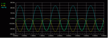
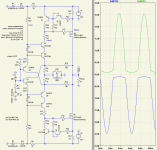
As long as you stay within class A limits, not only the voltage has low distrtion, but also the current in both halfs. When you move to class AB, of course the currents will tend to bend towards half wave rectified shapes. But you should subtract both current halves from each other, for that is the output current. Then the distortion will be typically lower than fixed bias class AB. See attached waveforms, showing top and bottom currents and their difference.
Anyway the output is non-switching, which is a good thing.
From my point of view it was neither about class A sound, nor about lowest output stage distortion. Just a class A output stage with the possibility of additional output current by moving to class AB, still non-switching and without bias adjustments and thermal runaway.
Steven
Hi Bonsai,
Please re-read my first post of this thread. This circuit is intended for class A amplifiers, with the possibility to move to class AB in case excessive currents are needed.
As long as you stay within class A limits, not only the voltage has low distrtion, but also the current in both halfs. When you move to class AB, of course the currents will tend to bend towards half wave rectified shapes. But you should subtract both current halves from each other, for that is the output current. Then the distortion will be typically lower than fixed bias class AB. See attached waveforms, showing top and bottom currents and their difference.
Anyway the output is non-switching, which is a good thing.
From my point of view it was neither about class A sound, nor about lowest output stage distortion. Just a class A output stage with the possibility of additional output current by moving to class AB, still non-switching and without bias adjustments and thermal runaway.
Steven
Attachments
dimitri said:dear Steven,
I like to read your posts very much but it seems that you spend too much efforts trying reinvent the wheel
S.Tanaka, "New Biasing Circuit for Class B Operation," JAES, 1981, Vol. 29, No 3, p. 148
Fifteen years ago I also was that optimistic and try to check as much as possible. Pity to say but 90% of my prototyping time was waste as somebody else did it before.
Hello Dimitri
I develop Stevens schematic 1986 after I see/test Tanakas design.
Since then all my source followers with big source resistors for shure paralleling worked with it.
For a high power bandwidth (< 1Mhz) with low distortion it´s essential that the source current never go to zero.
The circuit works best if D1/6 combines the quality from a ic- shunt regulator with the speed of a 1N4448.
Sorry, I can´t post further details.
Regards,
Heinz!
Steven, I did read your thread carefully. I understand the class A to class AB transition will result in the half wave rectified shape you show. However, when I simulated, the class A current waveforms were not symmetrical and small changes in Vref (= the bias diode) cuased big changes in this waveform. Per my earlier mail, I could not reconcile the distorted current waveform with the clean voltage waveform.
Regards
Regards
Re: new MOSFET biasing
Hello Anli,
looks interesting, nice work!
All 3 seem to be transconductance amps with feedback.
Will be nice if you can post the LTspice files together with the models here (zipped)....so the lazy ones like me can test it easy!
Regards
Heinz!
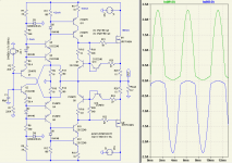
anli said:Have designed new MOSFET biasing. Three use cases (drafts) are below.
First one:
Hello Anli,
looks interesting, nice work!
All 3 seem to be transconductance amps with feedback.
Will be nice if you can post the LTspice files together with the models here (zipped)....so the lazy ones like me can test it easy!
Regards
Heinz!
Re: Re: new MOSFET biasing
Here it is. Also modified LTspice's lib/cmp files are included.
powerbecker said:
Hello Anli,
looks interesting, nice work!
All 3 seem to be transconductance amps with feedback.
Will be nice if you can post the LTspice files together with the models here (zipped)....so the lazy ones like me can test it easy!
Regards
Heinz!
Here it is. Also modified LTspice's lib/cmp files are included.
Attachments
Re: Re: Re: new MOSFET biasing
Thank you very much, I´ll try them later!
anli said:
Here it is. Also modified LTspice's lib/cmp files are included.
Thank you very much, I´ll try them later!
Anli,
please can you explain how to get the nice pictures from Ltspice
you post here?
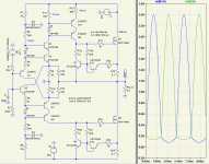
All your circuits are transconductance amps with FB so I take the best (the simplest, with THD20=0.23% ) for some improvements.
I add 2 drivers ,now all have a power bandwidth of 1MHz,
the simplest one has a THD20=0.01% which is fairly low for such a simple schematic !
Also I try to add a AD8099 for further FB, and at least the inverting example goes down to 0.000 12% without loosing the bandwidth.
Of course that´s only simulations but I am fairly confident that the behaviour in reality will be similar.
Thanks for your nice idee!
Regards
Heinz!
please can you explain how to get the nice pictures from Ltspice
you post here?
All your circuits are transconductance amps with FB so I take the best (the simplest, with THD20=0.23% ) for some improvements.
I add 2 drivers ,now all have a power bandwidth of 1MHz,
the simplest one has a THD20=0.01% which is fairly low for such a simple schematic !
Also I try to add a AD8099 for further FB, and at least the inverting example goes down to 0.000 12% without loosing the bandwidth.
Of course that´s only simulations but I am fairly confident that the behaviour in reality will be similar.
Thanks for your nice idee!
Regards
Heinz!
Attachments
Heinz,powerbecker said:Anli,
please can you explain how to get the nice pictures from Ltspice
you post here?
All your circuits are transconductance amps with FB so I take the best (the simplest, with THD20=0.23% ) for some improvements.
I add 2 drivers ,now all have a power bandwidth of 1MHz,
the simplest one has a THD20=0.01% which is fairly low for such a simple schematic !
Also I try to add a AD8099 for further FB, and at least the inverting example goes down to 0.000 12% without loosing the bandwidth.
Of course that´s only simulations but I am fairly confident that the behaviour in reality will be similar.
Thanks for your nice idee!
Regards
Heinz!
1. You have not set mosfet current to something about 150-200mA (with simply added follower you have ~2.7A).
2. I'm not sure THD itself does mean too much.
anli said:
Heinz,
1. You have not set mosfet current to something about 150-200mA (with simply added follower you have ~2.7A).
2. I'm not sure THD itself does mean too much.
OHHH, sorry, you are right how awkward!!

Please don´t look at my simulations!!
Now I changed 4 resistors and test the circuits again with 200mA quiescence current.
And of course bandwidth and distortion gets a bit worse.
When I added the driver I don´t realize, that a adjustment for different Gate-Source voltages would be necessary.
I hope I´ve done no further mistakes.
Heinz!
And of course bandwidth and distortion gets a bit worse.
When I added the driver I don´t realize, that a adjustment for different Gate-Source voltages would be necessary.
I hope I´ve done no further mistakes.
Heinz!
Attachments
- Status
- This old topic is closed. If you want to reopen this topic, contact a moderator using the "Report Post" button.
- Home
- Amplifiers
- Solid State
- New class A biasing (with non-switching class AB overflow)