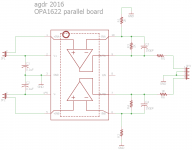
stackable parallel boards
I think that I'm going to parallelize the OPA1622's by stacking boards.
Each board is 25mm x 30mm, just $1.60 each at pcbway.com for 10 (plus ship). I've included a (1R) series resistor on each output. If I use collet socket headers I should be able to stack the boards. Two boards gives two in parallel on each channel. 4 boards would give 4 in parallel on each channel, the minimum for good audio (kidding...).
Part of the thinking here is the OPA1622's package is something I just absolutely don't want to solder. By making a small board with minimal parts I can get a quote on professional assembly by the board house. Then I can plug the stack into a larger DIY-friendly board that has the jacks, pot, batteries, and all the other good stuff. With 600pF drive capability I'm expecting that the chip won't have oscillation problems with the header/interconnect capacitance.
The amps are set up as non-inverting, of course. The ground return resistor for the parallel non-inverting input would be on the main board, similar to the O2 headamp's output section
If I do have it professionally stuffed I could swap out the 0805 sized parts here to 0603, 0402, or other eye-crossingly-small SMD types.
I think that I'm going to parallelize the OPA1622's by stacking boards.
Each board is 25mm x 30mm, just $1.60 each at pcbway.com for 10 (plus ship). I've included a (1R) series resistor on each output. If I use collet socket headers I should be able to stack the boards. Two boards gives two in parallel on each channel. 4 boards would give 4 in parallel on each channel, the minimum for good audio (kidding...
).Part of the thinking here is the OPA1622's package is something I just absolutely don't want to solder. By making a small board with minimal parts I can get a quote on professional assembly by the board house. Then I can plug the stack into a larger DIY-friendly board that has the jacks, pot, batteries, and all the other good stuff. With 600pF drive capability I'm expecting that the chip won't have oscillation problems with the header/interconnect capacitance.
The amps are set up as non-inverting, of course. The ground return resistor for the parallel non-inverting input would be on the main board, similar to the O2 headamp's output section
If I do have it professionally stuffed I could swap out the 0805 sized parts here to 0603, 0402, or other eye-crossingly-small SMD types.
Attachments
Last edited:
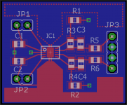
I'm looking at your layout, and the R and C in the feedback loop are just as shown on the datasheet page 26.I think that I'm going to parallelize the OPA1622's by stacking boards.
The data sheet says:
"Place the external components as close to the device as possible. As shown in Figure 60, keep feedback resistors close to the inverting input to minimize parasitic capacitance and the feedback loop area."
This may be picking nits, but I've seen elsewhere that such small things can make a difference. It looks to me that the higher frequency currents (that are more liable to be radiated and such) go through the feedback capacitor (C3 and C4 on your layout) rather than the resistor (R3 and R4), and so it should be the capacitor that's closest to the opamp's output and negative input terminals, not the resistor.
On the datasheet layout it says "Place feedback resistors to minimize feedback loop area." That's certainly correct if there's only a resistor in the feedback loop, but I'd change that text to say "Place feedback COMPONENTS to minimize feedback loop area" and the component conducting the highest frequencies should be closest to the opamp.
The OPA1622 is used in the Fiio E17K
I did some net searching to see if I could find any commercial products using the OPA1622 yet. One turned up, the Fiio E17K portable DAC/headamp that includes a battery:
FiiO-Born for Music and Happy
Curious thing though, they are apparently using the 1622 as the DAC LPF but using a (OPA1642 + LMH6643) pair for the output buffer.
I've puzzled over that a bit, why they didn't just take the output from the OPA1622 directly. Maybe the output stage has gain and they didn't want to try adding gain to a 2nd or 3rd order active LPF.
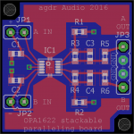
I cleaned up the parallel stackable board a bit, 25 x 25mm now, and converted to 0603 sized stuff. Clicking on the lower left corner will zoom it up quite a bit. I've also received an assembly quote that it is not too bad, $150 for any amount of boards up to 50 or so. If this thing works when it gets back and tested I'll start a thread in the headphone forum here.
A big thanks to johnc124 for all the helpful information!!
I did some net searching to see if I could find any commercial products using the OPA1622 yet. One turned up, the Fiio E17K portable DAC/headamp that includes a battery:
FiiO-Born for Music and Happy
Curious thing though, they are apparently using the 1622 as the DAC LPF but using a (OPA1642 + LMH6643) pair for the output buffer.
I've puzzled over that a bit, why they didn't just take the output from the OPA1622 directly. Maybe the output stage has gain and they didn't want to try adding gain to a 2nd or 3rd order active LPF.
I cleaned up the parallel stackable board a bit, 25 x 25mm now, and converted to 0603 sized stuff.
Clicking on the lower left corner will zoom it up quite a bit. I've also received an assembly quote that it is not too bad, $150 for any amount of boards up to 50 or so. If this thing works when it gets back and tested I'll start a thread in the headphone forum here. A big thanks to johnc124 for all the helpful information!!
Attachments
Last edited:
The E17K was released a year before the OPA1622 was created. I believe it was a typo in their original marketing material, but once it's on the internet, it's there forever.
Benb: You make a valid point about placing the capacitor closer to the chip to shrink the feedback loop at high frequency.
Benb: You make a valid point about placing the capacitor closer to the chip to shrink the feedback loop at high frequency.
Lol, leave it to Fiio to "use" a chip that doesn't exist yet. The link is right to their webpage. They still haven't corrected it after all this time.
John - could you provide any pointers to any publically announced/released headphone amps with the chip? I'm sure there is a bunch of stuff in development under NDA, I'm just curious if anything has been released yet. Thanks!
Whoops, I just realized that benb's helpful comment there was for the board stack. He was posting while I was composing! Thanks guys, I will take a look at that. I should swap R3/C3 & R4/C4.
Also, a question for John or anyone else out there with a boatload of layout experience. Would removing the soldermask over the two end-fire heat sink foil areas dissipate more heat than if they were covered with soldermask?
The link is right to their webpage. They still haven't corrected it after all this time. John - could you provide any pointers to any publically announced/released headphone amps with the chip? I'm sure there is a bunch of stuff in development under NDA, I'm just curious if anything has been released yet. Thanks!
Whoops, I just realized that benb's helpful comment there was for the board stack. He was posting while I was composing! Thanks guys, I will take a look at that. I should swap R3/C3 & R4/C4.
Also, a question for John or anyone else out there with a boatload of layout experience. Would removing the soldermask over the two end-fire heat sink foil areas dissipate more heat than if they were covered with soldermask?
Last edited:
I've puzzled over that a bit, why they didn't just take the output from the OPA1622 directly. Maybe the output stage has gain and they didn't want to try adding gain to a 2nd or 3rd order active LPF.
Looks like they could have saved themselves a chip by building an MFB lowpass filter around the composite pair. MFB can be arranged to have gain.
Good point! I can't remember if adding the two gain resistors to the MFB messes with the filter math or if it is independent. Regardless they should have been able to compute it easily enough.
3rd order Multiple feedback Low-pass Filter Design Tool
3rd order Multiple feedback Low-pass Filter Design Tool
I'm not sure if anyone is offering a publicly released product with the OPA1622 at this time. I can update this thread when someone makes an announcement that explicitly states they are using it. Overall I would prefer to keep this thread focused on technical discussions and questions about the part that I can help answer.
Remember, the OPA1622 was released to the market mid-December 2015, a little over 3 months ago. Bringing a (commercial) product to market takes time!
Remember, the OPA1622 was released to the market mid-December 2015, a little over 3 months ago. Bringing a (commercial) product to market takes time!
I can't remember if adding the two gain resistors to the MFB messes with the filter math or if it is independent. Regardless they should have been able to compute it easily enough.
If you go for gain you find your feedback cap gets smaller by the gain factor if I recall. Which kinda makes sense - the amp is a kind of amplified bootstrap multiplying up the value, like what happens in Miller compensation.
ordered some other boards
Just taped out my little test motherboard. It accepts the OPA1622 in the 10-pin, 300 mil DIP package, which I believe will probably be the most frequently used form factor for thru-hole adapters and daughterboards (example: post #76 in this thread).
It places four power supply bypass capacitors right at the pins of the opamp DIP: two electrolytic caps on the front (C2,C4) and two X7R ceramic 1uF caps on the back (C3,C5). Then the adapter daughter card itself has four more bypass capacitors.
50 ohm BNC jacks are provided, in case I ever want to try connecting it up to a spectrum analyzer or other super high frequency test equipment.
Will the very first revision work flawlessly? Highly doubtful. But we'll see.
_
Attachments
Last edited:
Mark - I think your board is going to be popular. Despite quite a bit of searching I haven't found an off-the-shelf (V)SON-10 breakout anywhere. Lol, Google did come up with this for "SON-10 breakout" though and I got a good laugh.
I'm designing an amp in another forum here that will use one of your boards, if the vertical dimensions work out.
I'm designing an amp in another forum here that will use one of your boards, if the vertical dimensions work out.
The board on post #76 needs to be modified to include a heat sink.
Whoops! You forgot to type "if the load impedance is below XX ohms" and you forgot to insert the value of XX that your calculations show to be prudent.
When OPA1622s are used in electronic crossovers, line-level preamps, audio mixers, etc., they drive load impedances of at least 2 Kohms and usually larger. With ±18V supplies, that's no more than 162 milliwatts* dissipated in each of the two output stages -- to deliver the necessary current to the 2K load. To that we must add 302 milliwatts of quiescent (bias) power: 4.2mA x 2 channels x 36 volts. Using the worst-of-the-worst case thermal parameters (58 C per watt), the junction temperature will be 36C warmer than ambient air with no heatsink. Which is quite acceptable.
For those who might wish to add a heatsink, you could consider the Assmann V5618A (link 1) whose mechanical drawing is (here). Price is USD 0.61 in quantity=1. As you would expect this increases the vertical height.
*this is a (loose) upper bound which is especially easy to calculate; those who prefer the more exact RMS calculation whose result is quite a bit less than 162mW/channel, are welcome to perform it.
Last edited:
Thank you, Mark, for your reply.
If you read post #1, the main reason for developing the 1622 chip is to drive headphones, most of which will have a low impedance. Limiting a mounting board for its use for 600 ohm and higher impedance devices does not make sense to me. Since the bottom of the chip has metal pad, I am assuming that the best place to remove heat from the chip is from this metal pad.
If you read post #1, the main reason for developing the 1622 chip is to drive headphones, most of which will have a low impedance. Limiting a mounting board for its use for 600 ohm and higher impedance devices does not make sense to me. Since the bottom of the chip has metal pad, I am assuming that the best place to remove heat from the chip is from this metal pad.
As N. Wolfe says to the League of Frightened Men (p.40), I only put that in so that you gentlemen would have something to take out.
Those who refuse to consider a topside heatsink, and who insist upon large area PCB copper pads, will need to abandon the idea of an 0.6 inch by 0.4 inch SMD-to-thruhole adapter board. You'll need to design a new adapter board whose area is much greater than 0.24 square inches, and you'll need to decide how to connect it to your thru-hole motherboard. Two rows of 5 pins is only one idea; you could also make a "quad", a square PCB with 4 pins along each edge, or a pin grid array with more than one row of pins per edge, or anything else your fancy might suggest. More pins means more mass and less thermal resistance between mother and daughter; it also means more male/female pairs needing mechanical alignment before mating. To anyone and everyone that decides to undertake the design and construction of such an adapter, I offer my sincere best wishes for rapid progress and good success.
On the other hand, those who wish to try the OPA1622 simply because it's an excellent dual opamp with wonderful specifications including tremendously low distortion, and who aren't going to use it to drive headphones, can get by just fine with an 0.6x0.4 adapter board and plain old IC sockets for 300 mil DIP packages.
Last edited:
To be perfectly honest I'd be surprised if anyone needed a heatsink for normal headphone use with anything resembling normal headphones. Low Z phones typically have very high sensitivity and need very little voltage to reach ear splitting levels, with high Z phones needing more voltage, but less current. Neither need much in the way of watts or device power dissipation whichever way you look at it. Only some esoteric headphones (as has already been mentioned) will probably require everything the device can supply, but only then if you decide to deafen yourself with sine waves.
The 1622 intrinsically has low quiescent currents so isn't going to get anything close to hot when doing nothing and therefore will have a lot of thermal headroom available for device dissipation when actually driving something.
The bottom line is that an 8pin DIP adaptor is going to be functional, stable and easy to use, which most people want. Buy one, whack it on a breadboard, give it a go, see if it suits your needs and if not then investigate a more substantial PCB or small top side heat sink.
From a purely engineering point of view though it would seem like there would be a requirement for two adaptors. One that makes it fit into the standard 8pin DIP dual layout. This would be for active xovers, line drivers, pre amp buffers, I/V stages, anything that a standard opamp would be used for. Then there would be a larger high power version, either complying to the 8 DIP pin layout but with overhang on the PCB for added dissipation, or with the PCB more resembling the natural layout of the 1622.
Clearly there would be a lot more demand for the smaller version as it would drive most peoples headphones too. No doubt if both versions existed most people would buy the high power versions for driving headphones, even if they didn't need it, but that's not the point. In the face of having only one option, the small 8 pin DIP is the way to go, especially as a top side heat sink will have the chip driving anything up to its current limit.
Very encouraging. Thank you 5th element and Mark for your input. I am going to try this, and will report.
I listen at modest levels. You have made the project easier.
I presume it is necessary to connect the bottom pad to the V-. A small wire attached to the side should do this if there is no solder pad under the bottom.
I listen at modest levels. You have made the project easier.
I presume it is necessary to connect the bottom pad to the V-. A small wire attached to the side should do this if there is no solder pad under the bottom.
Last edited:
- Home
- Vendor's Bazaar
- New Audio Op Amp - OPA1622