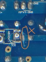
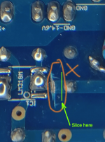
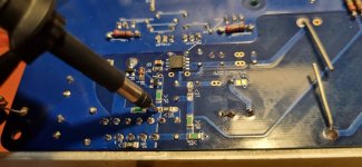
That's micro surgery!The above operarion illustrated
Could you say more about the change in sound?Would like to add that this mod changes the compensation in a measurable way. And also the sound, in my opinion in a remarkable way.
Gotta love the options for SMD rework. ") One suggestion: Instead of slicing the trace by the LM318, slice it closer to the through-hole part. You can then let the metal end of the SMD resistor sink into the solder on the PTH pad and solder the other end to the remaining trace. That allows the resistor to lay flat on the board, which is easier to work with and probably also more reliable (assuming you're not just hacking a quick prototype).
One suggestion: Instead of slicing the trace by the LM318, slice it closer to the through-hole part. You can then let the metal end of the SMD resistor sink into the solder on the PTH pad and solder the other end to the remaining trace. That allows the resistor to lay flat on the board, which is easier to work with and probably also more reliable (assuming you're not just hacking a quick prototype).
Tom
One suggestion: Instead of slicing the trace by the LM318, slice it closer to the through-hole part. You can then let the metal end of the SMD resistor sink into the solder on the PTH pad and solder the other end to the remaining trace. That allows the resistor to lay flat on the board, which is easier to work with and probably also more reliable (assuming you're not just hacking a quick prototype). Tom
Attachments
I'd be interested to hear your thoughts on that compensation mod too @Joseph K
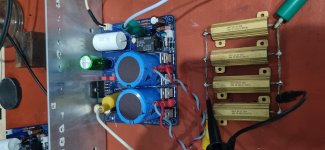
In the meantime my boards are lashed up and making noise with my disposable speakers. Fired up first time. Thank you Dario and all contributors! Will let them run before hooking them up to my main system.
In the meantime my boards are lashed up and making noise with my disposable speakers. Fired up first time. Thank you Dario and all contributors! Will let them run before hooking them up to my main system.
Hi all,
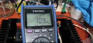
Did you have measure at pin#9 of LM3886? It have a sinewave signal with 524khz and Vpk-pk = 2V. I don't know, where it's come from? DC out measure is 11mV with signal input to gnd. It is same value of two boards.
Did you have measure at pin#9 of LM3886? It have a sinewave signal with 524khz and Vpk-pk = 2V. I don't know, where it's come from? DC out measure is 11mV with signal input to gnd. It is same value of two boards.
Attachments
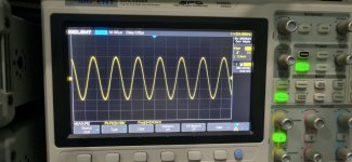
@vuthanh6 - hmm, I don't think it's a good idea to place your oscilloscope probe to pin 9, that is the inverting input pin of the LM3886 chip. at that point you have the full gain (close to 100db, enormous ); without any limitation on it. Your input signal is the pickup from your nice big extension antenna wire (scope probe) + common mode noise insertion from the scope grounding etc etc..
In fact, a quick way to induce your amp into oscillation is just placing your finger at that area..which is still a much more benign approach with respect to Your probe...
if you measured there 2V, then the output was already slewing like crazy rail to rail..
Also in general, never try this on any other opamp circuit with feedback. You should know deeply what you are up to for doing this. You can try to pick up that error signal, but you must design the local buffer circuit which isolates that extremely sensitive node with minimal influence, minimal capacitance, proper grounding etc..
And still then, in normal operation the maximal excursion at that point is expected to be less then millivolts, you will have difficulties to see that on a standard scope.
So it's a test which do not give a valuable result but risks your circuit's health in return..
Ciao, George
About my modification - I think it eliminates a little design feature that slipped the attention of the orherwise so great Mauro Penasa. The original idea, task of the C12 input capacitor together with R12 input resistor is / was RF input filtering so as to exclude input signals that are faster than the global loop reaction time.
in standard case that RC filter is placed on the +IN pin, where in fact it does not provoke any secondary effects, only the intended useful function.
In this special circuit instead, because of the double inverting gain structure, the global non-inverting input node ends up onto the -IN node of the control opamp.
At that position an extra 220pF local input load is heavily affecting the noise gain of the control opamp, it causes noise peaking and affects the high freq. phase response of that opamp.
Placing that 'damping' input resistance helps to separate these two effects, the intended input RF filtering effect, and unintended extra input capacitive load, causing noise peaking and phase alterations.
This separation then helps to obtain a cleaner, better defined behaviour when actually adding the extra compensation elements to the control opamp (like Cf at pin2, pin6).
I could then tell my tales about the sound effects but it will be subjective so maybe better restrain.. In think the technical reasoning is sound enough in itself..
Last edited:
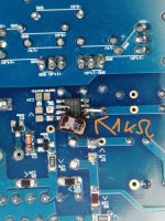
Response to Tom: yes, you are right, a classic standard lying flat position is better, safer for that resistor. My only little excuse that I had a relatively big size, 1206 resistor at hand, and with that size the sideways, narrow solder tab permitted a much cleaner approach when soldering amongst those SOIC pins.. Your suggestion will work better with a small, 0805 or even 0603 size. Best would be a small redesign?
Many thank Ciao, I learned more from you!@vuthanh6 - hmm, I don't think it's a good idea to place your oscilloscope probe to pin 9, that is the inverting input pin of the LM3886 chip. at that point you have the full gain (close to 100db, enormous ); without any limitation on it. Your input signal is the pickup from your nice big extension antenna wire (scope probe) + common mode noise insertion from the scope grounding etc etc..
In fact, a quick way to induce your amp into oscillation is just placing your finger at that area..which is still a much more benign approach with respect to Your probe...
if you measured there 2V, then the output was already slewing like crazy rail to rail..
Also in general, never try this on any other opamp circuit with feedback. You should know deeply what you are up to for doing this. You can try to pick up that error signal, but you must design the local buffer circuit which isolates that extremely sensitive node with minimal influence, minimal capacitance, proper grounding etc..
And still then, in normal operation the maximal excursion at that point is expected to be less then millivolts, you will have difficulties to see that on a standard scope.
So it's a test which do not give a valuable result but risks your circuit's health in return..
Ciao, George
I just simple think oscilloscope probe have 9M Ohm will be safe anywhere.How to reduce dc output voltage. Last time, I have used My-Ref version pcb (Aliexpess) only have 3.7mV dc output.
Attachments
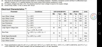
As You see, an LM318-N is having 4 mV typical, 10mV max guaranteed offset voltage declared. To this one should add the onboard leakage currents, multiplied for example by the 100kohm input resistance. I think your value is still completely in range... And it does not have any effect on your loudspeaker.
In the other board You had a different chip.
Anyway, the things to look for:
Chip differences;
leakage currents on the, around the -IN pin. (solder flux residuals- in the SMD version much more possibility for it than in the TH board)
maybe C9 leakage .. but this is not a primary effect
In the other board You had a different chip.
Anyway, the things to look for:
Chip differences;
leakage currents on the, around the -IN pin. (solder flux residuals- in the SMD version much more possibility for it than in the TH board)
maybe C9 leakage .. but this is not a primary effect
Attachments
I made Josephs modification yesterday, a 0603 fits nicely in the space, if a bit fiddly to fit. I'm very glad to report my experience: the technical improvement is indeed audible in a positive way! My faith in the laws of physics has not been challengedAbout my modification - I think it eliminates a little design feature that slipped the attention of the orherwise so great Mauro Penasa. The original idea, task of the C12 input capacitor together with R12 input resistor is / was RF input filtering so as to exclude input signals that are faster than the global loop reaction time.
in standard case that RC filter is placed on the +IN pin, where in fact it does not provoke any secondary...
I could then tell my tales about the sound effects but it will be subjective so maybe better restrain.. In think the technical reasoning is sound enough in itself..
Is this modification, inserting a resistor in the signal path between R12 and pin 2, appropriate for all varieties of opamps, including LM318?I made Josephs modification yesterday, a 0603 fits nicely in the space, if a bit fiddly to fit. I'm very glad to report my experience: the technical improvement is indeed audible in a positive way! My faith in the laws of physics has not been challenged
Dario, are you following this? Have you tried it? Can you, or anyone else, elaborate on the sonic benefits?
Peace,
Tom E
Tom, sorry for the delay..
I don't think much people could have tried this mod yet, if not some of the friends in our circle.
Though typically with the usual Fet input opamp versions.
I have a feeling that it could be interesting also with the original LM318.. maybe we can try it soon, with friends setups.
It does change the compensation parameters, so when applied it should be definitely 'controlled' for the correct response, and maybe adjustments needed.
Maybe I could come back with some results in a reasonable time..
All the best! George
Just to add some observations. In my original query about the value of C32 for my OPA828 build, @Joseph K intimated that with the damping resistor mod fitted 150pF would still be a valid value. I went ahead with the recommended 68pF, I then added the compensation damping 1K resistor which definitely dropped a veil in the presentation but there was still a hint of grit and grain in the 2-4kHz presence region, not surprising as it's something I've always heard in virtually all solid state amps. Only valves get those micro tonal shades in sibilants and cymbals absolutely right in my experience. Joseph's insight got under my skin, so I swapped out the 68pF for 150pF and nearly all of that grit and grain vanished. OK, I swapped a polystyrene for an AMCH and I am just a tinkerer but I do believe Joseph is on to something here.About my modification - I think it eliminates a little design feature that slipped the attention of the orherwise so great Mauro Penasa. The original idea, task of the C12 input capacitor together with R12 input resistor is / was RF input filtering so as to exclude input signals that are faster than the global loop reaction time.
in standard case that RC filter is placed on the +IN pin, where in fact it does not provoke any secondary effects, only the intended useful function.
In this special circuit instead, because of the double inverting gain structure, the global non-inverting input node ends up onto the -IN node of the control opamp.
At that position an extra 220pF local input load is heavily affecting the noise gain of the control opamp, it causes noise peaking and affects the high freq. phase response of that opamp.
Placing that 'damping' input resistance helps to separate these two effects, the intended input RF filtering effect, and unintended extra input capacitive load, causing noise peaking and phase alterations.
This separation then helps to obtain a cleaner, better defined behaviour when actually adding the extra compensation elements to the control opamp (like Cf at pin2, pin6).
I could then tell my tales about the sound effects but it will be subjective so maybe better restrain.. In think the technical reasoning is sound enough in itself..
First of all: Simon, thanks for your report!
I can only quote your observation. And I'm happy that it was not me, that I stayed put about the sound. And still you found something similar to me..
Dan, let me reassume:
Original suggested config for OPA828:
extra 5pF accross pin2-pin6, 68pF main compensation cap (C32),
R39, R43, C10, C34 eliminated
New modified compensation for OPA828:
extra 5PF accross pin2-pin6, 150pF main compensation cap (C32), 1kohm inserted between C12(220pF input cap) & pin2 (-IN)
R39, R43, C10, C34 eliminated
That intermediate solution Simon talked about was just a temporary, intermediate 'trial' solution from his part
All the best, George
- Home
- Amplifiers
- Chip Amps
- My_Ref Fremen Edition - Build thread and tutorial