Not a silly question at all. That's exactly what I did with my SOMA2 (A glorified DC coupled szekeres with gain), both CCS and source follower user IRF620s. In all honesty I don't think there's a huge gain in both being the same part, as the FETs are being used in different capacities. So long as your follower keeps following and your CCS remains constant, the circuit will keep working. If getting a more constant CCS requires using a different FET from the follower, go for it.
Mike.
Mike.
I'll throw it up for you this evening.
In the mean time I believe I owe AndrewT an apology, I believe his extra 0.7 derating factor may have been added in order to compensate for the pulsed current nature of cap charging rather than a repeat of the RMS/Peak correction.
0.7 is a rather arbitrary factor which is better determined through simulation. Even with constant output of 1.6A the peaky nature of the bulk caps charging means the RMS current drawn from the transformer will be somewhat larger.
Sorry for the hasty reply and confusion caused.
Mike.
... I believe his extra 0.7 derating factor may have been added in order to compensate for the pulsed current nature of cap charging rather than a repeat of the RMS/Peak correction ...
in fact, simulations show Irms=4.6A and Ipeak=18A.
... If you ever decide to post it you'll have at least one reader!
make that two.
") mike, how did you stabilize the output offset of your amp with temperature? many have complained of high dc offsets with the plain-jane dc-coupled szekeres...
mike, how did you stabilize the output offset of your amp with temperature? many have complained of high dc offsets with the plain-jane dc-coupled szekeres...Just thinking out loud...
actually a very good question. as a matter of fact, i asked it myself when designing this amp initially. simulated distortion figures were better with an IRF640 in the ccs fet position instead of an IRF610.
~ brad.
I posted the schematic last night. You can find it here:
http://www.diyaudio.com/forums/headphones/163686-simple-op-amp-mosfet-amplifier-soma-2-a.html
DC offset was corrected by moving the output inside the feedback loop used for setting the gain.
I limited the RMS current in my power supply with a small resistor between the bridge rectifier and the bulk caps, you'll be surprised how little you need to really reduce the peaks. You'll have to take into account the voltage drop across it though. I use an 18V transformer to supply a 15VDC load.
thanks mike for the link. interestingly enough, the reason i decided not to pursue an M^3-like design was its push-pull nature, but your design fixes that by combining se class-a with the buffered opamp topology... it seems i won't be satisfied until i've built one and listened thoroughly...
also, i've been simulating with lateral mosfets in place of the irf610 in the szekeres design, and the results are quite interesting. for one, the frequency response (both ends, esp. hf) is extended. obviously gain is increased due to the lower Vgs(th) values. but most interesting, the harmonic distortion 'character' looks at first glace to be more pleasing, with the same amount of 2nd harmonic and greatly decreased 3rd and up harmonics...
i've been simulating with the 2sk216, but its 500mA Id(max) isn't cutting the mustard (or muster... w/e, lol), so i'm going to look at the 2sk1058 in the sim next.
the obvious result of all this is a delay in pcb design until i can simulate and breadboard each design and find a clear victor.
~ brad.
looks like the 1058 is a no-go
ok, i've simulated the 2sk1058 in the circuit and fiddled with optimum component values...
interestingly, the 2sk1058 performs much worse in frequency and phase response than any of the other mosfets. it does halve thd and present a nice distortion character, but hf response is ugly...
the next step is to look into (simulate) each of these mosfets (irf610, 2sk216, 2sk1058) in the SOMA2 circuit and see how they stack up there.
~ brad.
it's been a while, lol
so everybody knows, i haven't stopped working on this!
thanks to graduation, and now grad school, i've had little time (and money) to pursue this any further. but i have been able to simulate some designs which closely resemble the SOMA2. after looking closely at a few opamp/fet combinations, i've landed on the ad843 and 2sk216 as an optimal combination. i'm currently revising my schematics for this "v2" design.
the reason i'm going this direction is pretty basic: the trend in my latest szekeres amps was higher current -> lower thd, but it was getting a tad ridiculous. the v2 design ensures lower thd (thanks to the SOMA idea of moving the output FET into a GNFB loop) at lower dissipated power.
this does bring up an interesting question. these lateral fets seem to be made from unobtanium... any ideas where i can find them at a reasonable price? (borbely seems to be one)
i'll have a pdf up soon, hopefully.
~ brad.
Don’t know enough to comment deeply on the circuit, except to say that your op-amp needs a path to ground for the positive input to draw current.
Also, consider using a similar type of FET for the CCS, as this should theoretically help drift and give the op-amp a better chance of maintaining zero output offset.
Your positive shunt power supply makes sense, but you don’t really need the negative supply shunt because the amp circuit CCS already provides good PSRR to the negative supply. I think a simple three terminal regulator should be fine in the negative side. I know the supply will ‘look unbalanced’, but the amp circuit already is, so don’t be concerned!
Ampslab seems to have parts: 2SK1058 RENESAS/Hitachi Audio Power Mosfet - Buy Online @ AmpsLab
Don’t know enough to comment deeply on the circuit, except to say that your op-amp needs a path to ground for the positive input to draw current.
i'm not exactly sure what you mean. the opamp output has a (high-impedance) dc path to ground through the mosfet gate and an ac path to ground through the 33pF capacitor...?
Also, consider using a similar type of FET for the CCS, as this should theoretically help drift and give the op-amp a better chance of maintaining zero output offset.
i'll be sure to simulate a FET in the CCS position... an interesting thought.
Your positive shunt power supply makes sense, but you don’t really need the negative supply shunt...
well, i suppose a bit of overkill can't hurt, eh?
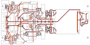
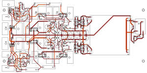
(i just read this as i finished the first revision pcb...)speaking of the pcb, i've attached it. it's a first-run, so it's not perfect, i'm sure... any glaring mistakes that i've missed through my all-day pcb brainstorm?
thanks,
~ brad.
Attachments
Your positive op-amp input needs to be able to source current from somewhere, and at the moment that is from whatever source you use, but only if it is DC coupled. When you disconnect the signal input of your circuit, or if the source is AC coupled, then there is no-where to source current from and that may result in a large DC offset at the output of the op-amp.
Every non-inverting op-amp circuit that I have seen has a permanent way for the positive op-amp input to receive current, normally via a resistor to ground (to the left of your series input resistor).
I think this is less of an issue with FET input op-amps, but still a consideration.
Every non-inverting op-amp circuit that I have seen has a permanent way for the positive op-amp input to receive current, normally via a resistor to ground (to the left of your series input resistor).
I think this is less of an issue with FET input op-amps, but still a consideration.
input resistors
alright, here's the updated schematic, layout and bom with input resistors. any comments? the pcb feels like a hack-job to me, for some reason, though i'm confident in the schematic design (and bom for that matter).
any layout nazi's out there?
~ brad.
alright, here's the updated schematic, layout and bom with input resistors. any comments? the pcb feels like a hack-job to me, for some reason, though i'm confident in the schematic design (and bom for that matter).
any layout nazi's out there?
~ brad.
Attachments
Last edited:
geekysauvo,
nice build log. i am planning on building a bog standard Szekeres with the intent to tweak the circuit as you have. i'm going to start off with a regulated single rail 24V PS (o11 The σ11 Regulated Power Supply), and then convert to a DC coupled with the remote dual-rail unregulated PS from my F5 and a o22.
i have an M3, B22, and Bijou (tube) as well.
thanks for taking the effort to detail your project
thanks for taking the effort to detail your project
thanks for the interest! let me know what you think of the szekeres.
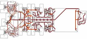
ok, here is a redesign of the current circuit. circuit and component changes are minimal aside from different zener diodes and half the number of regulator ccs fets.
i spent a bit more time trying to make the layout better, so hopefully it's less awful this time around. i'll be ordering parts pretty soon, as long as i can bring myself to spend the money. until then, please add any advice or ask questions.
~ brad.
Attachments
Oh my. The Szekeres amp is over 25 years old !!
a grand (perhaps late) happy birthday to the szekeres amp and many happy days for all its siblings and children!
thanks for the encouragement! i'm honoured that you've read the thread.i just started the parts ordering process for this design and i'll be tweaking the pcb as they come in, to make sure everything will fit.
some quick simulation values:
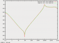
THD@1kHz/1Vpp(in): 0.00014%
THD@20kHz/500mW(out)*: 0.0047%
Phase shift@20kHz: -0.5 degrees
Freq Resp@0dB,-3dB: 0Hz-2.5MHz
Gain: 3V/V
* = The maximum input power for my HD595's
these values are surely overzealous, since they come from a simulation, but i'll be happy if the amp performs an order of magnitude worse than the simulated THD specs, honestly.
~ brad.
- Status
- This old topic is closed. If you want to reopen this topic, contact a moderator using the "Report Post" button.
- Home
- Amplifiers
- Headphone Systems
- my take on the szekeres