Hi all.
I freshly registered here and I would like to start posting with an introduction to my amplifier project. The name of the project is simply "MyAmp2006".
After months of reading books (D. Self, R.Slone, ...). I am still in the design and simulation phase. I use the free "SwCAD III" from LT for that.
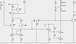
This is the latest version of my concept:
It's a 120W@8Ohms BJT class B design using three paralleled pairs of OnSemi's ThermalTrak output devices (which I got already as samples).
Results of simulation:
max input level: 2.828V (output 120W@8Ohms)
min input level: 0.044V (output 30mW@8Ohms)
DC offset: -22µV
slew rate: 54 V/µs (symmetric)
bandwidth (-3dB): 2Hz to 400kHz
output noise: 63nV/sqrt(Hz)
quiescent current through each output device: 10.6 mA.
These are THD values by simulation:
What do you think about this design? Do above numbers look acceptable?
During simulation, I could not see any signs of instability. Do you see any instability or blow-up risks with my concept?
I would like to omit the usual output current sensing and limiting, just keeping the rail fuses. Each of the three paralleled output devices should withstand max 15A (by datasheet). 3x15A is much more than my transformer can do. Thus, rail fuses of 10A or so should make it. Do you agree?
Thanks for having a look on it.
Regards,
mafoe
I freshly registered here and I would like to start posting with an introduction to my amplifier project. The name of the project is simply "MyAmp2006".
After months of reading books (D. Self, R.Slone, ...). I am still in the design and simulation phase. I use the free "SwCAD III" from LT for that.
This is the latest version of my concept:
An externally hosted image should be here but it was not working when we last tested it.
It's a 120W@8Ohms BJT class B design using three paralleled pairs of OnSemi's ThermalTrak output devices (which I got already as samples).
Results of simulation:
max input level: 2.828V (output 120W@8Ohms)
min input level: 0.044V (output 30mW@8Ohms)
DC offset: -22µV
slew rate: 54 V/µs (symmetric)
bandwidth (-3dB): 2Hz to 400kHz
output noise: 63nV/sqrt(Hz)
quiescent current through each output device: 10.6 mA.
These are THD values by simulation:
An externally hosted image should be here but it was not working when we last tested it.
What do you think about this design? Do above numbers look acceptable?
During simulation, I could not see any signs of instability. Do you see any instability or blow-up risks with my concept?
I would like to omit the usual output current sensing and limiting, just keeping the rail fuses. Each of the three paralleled output devices should withstand max 15A (by datasheet). 3x15A is much more than my transformer can do. Thus, rail fuses of 10A or so should make it. Do you agree?
Thanks for having a look on it.
Regards,
mafoe
Hi - looks good; how did you verify stability? Try kicking it with square wave inputs and a reactive load... Also, the rising THD vs lowering frequency (0.01% 150Hz and lower) seems odd...
Cheers!
ps: try dropping the bias currents and see if the simulation tallies. I would have thought 10mA is a bit low, so I'm wondering how 'true' the simulations are...
Cheers!
ps: try dropping the bias currents and see if the simulation tallies. I would have thought 10mA is a bit low, so I'm wondering how 'true' the simulations are...
Good to see someone is trying the Thermaltrak transistors out!
A question for you:
You said that your output devices are biased at 10.6ma per device. What is your method for adjusting the bias current since there is no Vbe multiplier adjust? (Sorry if the answer is in your schematic; I can open the link to your schematic but I can't see the schematic picture itself).
Hi,
I got several people reporting that the schematics is difficult to see. After clicking the thumbnail link, a strangely compressed view of the big picture appears. This picture can be zoomed in to see all details by simply left-clicking. Sorry, it's not my invention, seems it's how the "xs.to" image hosting site is dealing with images of huge size.
Back to my project:
to check stability, I fed the input with square waves up to maximum magnitude (+2.828V, -2.828V), with 1ns rising and falling edges. Even having set the max timestep of the Spice transient analysis down to 10ns I cannot see signs of voltage over-shoot or ringing at V(SPEAKER) output. Should I check something more?
THD: At the beginning I simulated only at 1kHz and 20kHz with full power, assuming that all other values at lower input freqs and levels would be equal or below. (maybe I misunderstood Mr. Randy Slone in his book High-Power Amplifier Construction Manual.) When I started to simulate a bit more to fill such THD table, I detected that my original design showed several weak spots in this table, e.g. like 0.03% at 2400Hz, 0.177V input, but having good 0.00x values in all the cells around. Yet, do not understand the mechanism that leads to this effect.
After weeks of playing around I found that the capacitor to buffer the V_bias (made by 4 ThermalTrak diodes) plays some role. I tried values of 1µF to 220µF, but this lead only to a shift of the bad points in the THD table. My latest approach with several small capacitors along the V_bias diodes improved the figures significantly. I don't know why.
The setup is not yet optimized. I took the 2.2n along the diodes just like that. I'll continue to find better values, and I will try to tune the quiescent current by adjusting the R11/R33/R34 chain. You said 10mA could be a bit low. Which value would you assume?
mafoe
Hi mafoe,
You may be chasing simulation gremlins. When spice-like simulators begin to give you funny values (i.e. changing capacitors that shouldn't have any effect but does!), then you can make a guess that it's time to go to a real-world breadboard....
Regarding bias - I believe D Self does some in-depth analysis and shows that its not really the current that counts but rather resulting bias voltage as measured (I'm just recalling here, please check the chapter to make sure) from the emitter resistors. Therefore, the lower the emitter resistor value, the higher the resulting "correct" current for bias. In your case, you've chosen 0.1ohm resistors, so I expect the "correct" bias current to be pretty high. Of course, this is on the assumption that D Self is correct.
On the other hand, most designers seem to favor bias per stage at 25 to 100mA... (other guys and gals, correct me if my memory is faulty!!)
Cheers!
Regarding complementary differentials with mirrors:
You're walking on the thin ice man, in sims all transistors of the same make are identical, in reality not allways.
Try simming 2 different transistors in differential pairs, like mpsa06 with 2n5551 and mpsa56 with 2sa970 and slightly different emitter resistors (+-5%). Try several times with differnt setups (hint: currents in VAS, balance) and don't be angry on me if you get dissappointed, sorry.
Hi, Mafoe,
Welcome to the forum
I've built this, and it doesn't work AT ALL in real cct. I don't know why it works in SIM.
Mafoe, try to replace the current mirrors with plain R, then it will work in real cct.
Welcome to the forum
Regarding complementary differentials with mirrors:
I've built this, and it doesn't work AT ALL in real cct. I don't know why it works in SIM.
Mafoe, try to replace the current mirrors with plain R, then it will work in real cct.
Hi mafoe,
One other thing I forgot, that you may want to try - put in "funny" values for the compensation capacitors in the amp, and load it with a reactive load. The objective - make the amplifier oscillate in simulation!!
If it doesn't oscillate, then you know the simulation can't be 100% believed... (ugh, ask me why I know...)
Cheers!
Clem
There is nothing to define the current of VAS stage in this circuit.
Not as far as I can see ....
Maybe I do not understand the idea of this circuit.
I have not seen this before.
I am talking about:
R19, R16, Q9 and Q12.
see detail in my attachment
Not as far as I can see ....
Maybe I do not understand the idea of this circuit.
I have not seen this before.
I am talking about:
R19, R16, Q9 and Q12.
see detail in my attachment
Attachments
Hi,
thanks for your interest and hints!
The roots of my project can be found in the book of Randy Slone that I mentioned above (ISBN 0-07-134119-6), on page 351. The differential input stage with current mirrors is almost copy&paste from there, including the values of the degeneration resistors. This gives me some confidence that it works. Since my rails run on lower volage (48V instead of 55V in the book) I substituted the 2N5551/2N5401 with MPSA06/MPSA56 types. A good choice?
The symmetric VAS is made of two Darlington circuits with active loads (whatever that means). In the original version in Slone's book, the cascode transistors (like Q9) are biased by a 4.4V zener diodes, each connected to its near rail. All my Spice simulations (Orcad/PSpice as well as SWCad III) had heavy convergence problems with that. So I finally decided to get rid of the zener and find another way of biasing the cascode. After trying funny circuits showing more oscillation than amplified signal, I came to the version that I posted here. I have not yet completely understood how this symmetric cascode thing works. Honestly, I don't know what defines the VAS current. I just see in the simulation that there is some current (about 45mA).
I'm on a business trip the rest of the week. I'll be back here on the weekend.
Greetings,
mafoe
mafoe said:
All my Spice simulations (Orcad/PSpice as well as SWCad III) had heavy convergence problems with that. So I finally decided to get rid of the zener and find another way of biasing the cascode. After trying funny circuits showing more oscillation than amplified signal, I came to
Convergence problems with Spice simulators usually mean that the circuit is oscillatory, that's one of the things I learned!
Have a nice business trip and keep us updated when you get back to your amplifier project!
Cheers!
Regarding bias - I believe D Self does some in-depth analysis and shows that its not really the current that counts but rather resulting bias voltage as measured ...snip... Of course, this is on the assumption that D Self is correct. ... snip ...(other guys and gals, correct me if my memory is faulty!!)
No your memory is fine, and it is not just D Self, a much earlier analysis by Gilbert I believe, and ... now my memory is getting vague ... there is a thread here at diyaudio about this, John Curl quotes something like put 15 to 25 mV across your emittor resistor. And of course I'm sure many others have done similar analysis, I've done it with spice and as the result of an almost constant voltage across the e resistors popped out my brain realised I'd just repeated something similar to Self's work (never bad to chceck) and later I read the thread with JC's quote, guess I was just reinvestigating the wheel, I guess that saying about learning from your own mistakes is true at times!
Bill
There is nothing to define the current of VAS stage in this circuit.
Not as far as I can see ....
Yup. There was a thread a year or two ago. The VAS simply won't turn on. Slone published 3 or 4 schematics somewhat like this and a number of thread members, including me, belived what the simulations seem to to say. But we all got sucked in. I don't get the impression Slone actually built his the designs; it may also be noteworthy that mirror imasge he did buld and variants of which are intended to be produced and sold by ZUS used cascodes instead.
I have speculated this is why Self does not use mirror image IS & VAS. After all, at first glance this would seem to his kind of circuit.
There are some very complex designs that force this approach to work by using diode clamps.
simulation can be the devil....
I'd say simulation is absolutely great tool. It can predict basic things, help you with sophisticated designs as well as help you to learn something from nearly scratch without burning silicon. Especially today it is very user friendly, no code, you just pick things and put together to see how stuff works.
Only, as every tool should be understood and user has to be aware of its severe limitations.
If one simulates slightly different bjts in design like this and shifts +-5% of resitors values everything gets clear...
Identical devices is one thing.
Other is weak predictions of stabiity and margins, especially with 'fast' designs with inproper realworld PCB.
There are some others also...
darkfenriz said:
Only, as every tool should be understood and user has to be aware of its severe limitations.
If one simulates slightly different bjts in design like this and shifts +-5% of resitors values everything gets clear...
Identical devices is one thing.
Other is weak predictions of stabiity and margins, especially with 'fast' designs with inproper realworld PCB.
There are some others also...
Agreed, and those "other things" may be the biggest problem, i.e. not modeling the parasitics of components, as well as the PCB layout...
Cheers!!
And then there are the designs that work, but only in real life and not in simulation, wish I could remember the circuit and a link or reference... you'll just have to take my word for it... I think it was a circuit explained and or designed by Pease, but I would not swear to it.
editted spelling - I need a new keyboard or I need to clean this one!
editted spelling - I need a new keyboard or I need to clean this one!
darkfenriz said:Regarding complementary differentials with mirrors:
You're walking on the thin ice man, in sims all transistors of the same make are identical, in reality not allways.
Try simming 2 different transistors in differential pairs, like mpsa06 with 2n5551 and mpsa56 with 2sa970 and slightly different emitter resistors (+-5%). Try several times with differnt setups (hint: currents in VAS, balance) and don't be angry on me if you get dissappointed, sorry.
Hi darkfenriz,
I tried what you said. You are right! Yes, I am disappointed now but not at all angry with you. I guess I'll rework my concept now and keep it a little more simple.
I was aiming for THDs of 0.000x all over the range of operation. Is that reallistic? Is that good enough? Is there any "golden" THD value one should stay below to name an amplifier "High-End"?
ciao,
mafoe
- Status
- This old topic is closed. If you want to reopen this topic, contact a moderator using the "Report Post" button.
- Home
- Amplifiers
- Solid State
- my project: class B with ThermalTrak