
From simulation with 100nF in the ic integrator I see a low frequency peak and with 10uF no peak.
What is the right compromise?
There's a little error in your sim schematic. R2 should connect to the negative rail and not to the output.
Try to adjust R21 together with the cap. And have an eye on the settling time, like @brian92fs said.
Meanwhile my amplifier is now set up in the living room, driving a pair of Infinity's. First impression is superb!
Finished
 !
!And the first impression still holds true. I am not good at answering the question of ''how does it sound?'', but I can say for sure that it sounds different than my other amplifiers, and it certainly sounds pleasing and not fatiguing! It has found its place in my main audio system, and it will stay there.
Some final photos (in rather bad lighting). The front panel was made by Schaeffer AG (or Front Panel Express, for those across the pond). It is anodized in a med-bronze color, which nicely matches the beige color of the case, as well as the champagne color of the Sony player next to it. I really like how it turned out!


And the first impression still holds true. I am not good at answering the question of ''how does it sound?'', but I can say for sure that it sounds different than my other amplifiers, and it certainly sounds pleasing and not fatiguing! It has found its place in my main audio system, and it will stay there.
And that is what it's all about. Good stuff
and a nice job Is there any reason not to use thicker wire for inductor?
I have some 1.25mm diameter magnet wire. Something in between AWG 16 and 17.
https://www.powerstream.com/Wire_Size.htm
According to the chart here, the skin effect comes into play here with:
"Maximum frequency for 100% skin depth for solid conductor copper" 11KHz for awg 16.
Is this something I need to worry about?
It depends on the load impedance because lateral FET's have a relatively high D-S channel resistance. In practice with music and driving a real typical 2 or 3 way speaker a single pair of single die FET's should get to within around 5 volts of each rail, the double die FET's a bit closer.
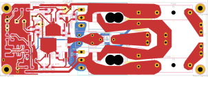
A few posts back, I uploaded Gerber/BOM, etc. for a 50mm width SMD version of Mooly's amp. Looking at the track widths for the MOSFETs, the current carrying ones have a track width of around 1.5mm which KiCad's calculator says will do 3.24A max. That should be OK for domestic use but doesn't have much margin so I've revisited the layout and beefed up the relevant tracks. I've also taken the opportunity to increase the size of the heatsink areas for the constant current and VAS transistors.A few posts back I uploaded the schematic and renderings for the revised layout with component numbering matching Mooly's original. I forgot to upload the Gerbers to go with it. Here they are if anyone cares to use them. I've just ordered a min quantity of 5 from JLCPCB so, once I extract 2 for myself, will have a couple spare and am happy to pass them on for cost of postage (within UK) if anyone is interested.
Attachments
- Home
- Amplifiers
- Solid State
- My MOSFET amplifier designed for music