I can't say I recall anything like that happening with mine.
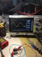
The actual trace is difficult to figure out. The scope trace should be a single 'line' and yet what you have here doesn't seem to correspond to that. The wanted signal rises cleanly andyet there is the noise showing as well. It is as if there are two traces at that point.

Have you tried altering the input frequency and scope triggering?
The actual trace is difficult to figure out. The scope trace should be a single 'line' and yet what you have here doesn't seem to correspond to that. The wanted signal rises cleanly andyet there is the noise showing as well. It is as if there are two traces at that point.
Have you tried altering the input frequency and scope triggering?
A thiele circuit added,no difference.
In this layout the WW resistors are in parallel and in intimate contact with each other - with ac currents passing through a wire which is spiral wound there will be radiated fields.
To avoid cross contamination between output halves through coupling effects these resistors should be spaced further apart. You could try wedging a thin strip of copper between these and solder this to a wire to earth through a small value capacitor and insulated wire.
There is no damping resistor for the output coil in the original circuit. JLH included such in his MOSFET design published in Electronics World + Wireless World in June 1993.
For the MOSFET outputs 2.5W rated Wire-wound source resistors would have been adequate.
If you replace the 5 Watt blocks with these narrower types and fit them with long leads so these can be bent further away from each other, and, include a damping resistor for the output coil, these steps could be enough to resolve the residual problem you are confronting.
Hi Mooly.I can't say I recall anything like that happening with mine.
The actual trace is difficult to figure out. The scope trace should be a single 'line' and yet what you have here doesn't seem to correspond to that. The wanted signal rises cleanly andyet there is the noise showing as well. It is as if there are two traces at that point.
View attachment 1114625
Have you tried altering the input frequency and scope triggering?
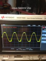
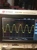
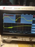
This happen at 20Khz.
At 10Khz clip is normal.
Same levels.
Attachments
Hi Mooly.
This happen at 20Khz.
At 10Khz clip is normal.
Same levels.
Hard to say tbh. It would be interesting to see that on an analogue scope with that part of the trace greatly expanded
 Whatever is there, the trace of the scope should only ever be a single line tracing out the signal. You might be chasing something that isn't real.
1)Analog scopeHard to say tbh. It would be interesting to see that on an analogue scope with that part of the trace greatly expanded
2)Digital zoom
Attachments
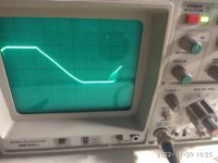
It looks like there is a high impedance condition in the biasing of the output stage. The waveform that you see is a result of the scope re-traces over many cycles of 10 Khz. The high impedance in the output stage may be modulated by noise from power supply radiation. Also, the output stage may have a local oscillation in its design that only occurs at certain bias conditions like in recovering from a clipping condition. The retrace envelope that you see is showing the boundary of the high impedance condition.1)Analog scope
2)Digital zoom
1)Analog scope
2)Digital zoom
Thanks
Interesting.I've no real ideas, only suggestions. Firstly, I'd have to at least say 'is this going to be a problem in use?" simple because clipping is outside the normal usage envelope anyway.
Obviously without having one in front of me... however... things I would try and all these years down the line and there are some things I might look differently on. The 0.22 ohms may not be strictly necessary. You could even try linking them out.
Could there be significant differences in the old original 2N5551's and 2N5401's I used all those years ago? I'm not sure what you used here.
The Exicon FET's should be direct substitutes and they are what others have used. Can't really see those being an issue.
Do you have to overdrive the amp significantly to see this issue or does it suddenly happen at the onset of clipping?
Hi Hicoco,no I haven't.Thimios did you check the signal @the gate of Q8 & Q9 to see how is the trace with the same signal @ the input ?
Do you mean at the same clipping levels?
Hi Mooly 5401&5551 that is used here manufactured by Unisonic.
No it doesn't happen in soft clipping conditions but in hard overdrive, about 560mV input signal.
Last edited:
Hi Mooly 5401&5551 that is used here manufactured by Unisonic.
No it doesn't happen in soft clipping condition but in hard overdrive, about 560mV input signal
Those should be fine.
I'm just playing with the simulation to see if I can get any clues and the only two things that provoke oscillation past the clipping point are if the 0.22 are quite inductive (10uH) which is massive for a low value resistor and also the 22pF cap if it happened to be a wrong value such as a 220pF. No other clues though.
That is what JLH wrote in his book on Valve and Transistor Audio Amplifiers although that was for a standard MOSFET pair not the compound circuit used by Mooly. His circuit resembles one by JLH in a HiFi News issue published in December 1980 -see attached.Hi prasi,glad to see you here!
Thanks for this pcb.
Please look at this picture.
Majona,do you recoment WW resistors instead of non inductance type?
In his book Valve and Transistor Audio amplifies JLH mentioned the use of inductive resistors in MOSFET output stages.
The small inductance in wire wound resistors value 0.22R in that example is to protect the Source electrodes of the MOSFETs.
With increasing frequency for the same level of current in the compound output stage, the local feedback due to inductance in R17 and R18 in JLH's circuit will increase above the local feedback level due to the drop across a non inductive resistor.
Resistors R17 and R18 have a nominal resistance of 0.47R -double the value of R23 and R24 in Mooly's circuit from which no inductive benefits accrue.
Ideally R19 and R20 (220R) should be deployed as JLH has shown R14 and R15 in his circuit. In that way the local feedback point of the compound pairs Emitter and Source see the identical feedback signal generated across the inductive resistors R17 and R18. This change would involve hacking the pcb or paying to have a new one made.
One could replace Mooly's R23 and R24 non inductive types with Wire wound to see how that goes. The problem with MOSFETs is their high frequency characteristics are far better than BJT devices and need a measure of taming whereas BJT devices under achieve and it is better not to limit their frequency response.
Attachments
I really don't know on that. The inductance of a low value wirewound is very small indeed and in my amp they are fitted to the Drain. Putting them in the Drian the way I have it reduces the transconductance of the whole output stage and the addition (or possible removal) of those is an area I would definitely look again at if I was doing this from scratch.
Try linking the resistors out. Use the bulb and there should be no risk. They play no part in the bias stability of the amp.
Strange to see no gate stopper resistors in that JLH.
This is when inductance is added to the Drain (my 0.22 ohms). This is also using models for the Exicon FET's. It shpws the potential for instability is there when inductance is present.

This is with the resistors linked out. Bias current hasn't altered at all.

Try linking the resistors out. Use the bulb and there should be no risk. They play no part in the bias stability of the amp.
Strange to see no gate stopper resistors in that JLH.
This is when inductance is added to the Drain (my 0.22 ohms). This is also using models for the Exicon FET's. It shpws the potential for instability is there when inductance is present.
This is with the resistors linked out. Bias current hasn't altered at all.
I will try to use no resistors and see the results.
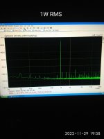
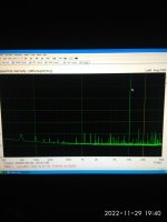
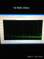
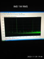
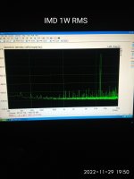
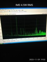
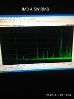
I have the THD measurements too.
I will repeat test if amplifier stay stable without resistors.
I have the THD measurements too.
I will repeat test if amplifier stay stable without resistors.
Attachments
-
 IMG_20221129_193902.jpg234.2 KB · Views: 76
 -
 IMG_20221129_194059.jpg201.4 KB · Views: 70
 -
 IMG_20221129_194341.jpg227.6 KB · Views: 63
 -
 IMG_20221129_194909.jpg218.9 KB · Views: 61
 -
 IMG_20221129_195047.jpg210.5 KB · Views: 64
 -
 IMG_20221129_195331.jpg279.9 KB · Views: 63
 -
 IMG_20221129_195511.jpg263.5 KB · Views: 61
 -
 IMG_20221129_193235.jpg209.7 KB · Views: 63
 -
 IMG_20221129_193640.jpg214.3 KB · Views: 71
Sorry about mixing up electrodes in my last post the drain is still an electrode. Just to change the subject a little if clipping is a problem on negative swings then there could be a problem with Q4 buffer level of current due to the value of R11 at 3k9 the collector of Q4 connects to zero volts. Is Q4 current level enough? 560 millivolt clipping seems to indicate a transistor in the negative half of the circuit is limiting.I really don't know on that. The inductance of a low value wirewound is very small indeed and in my amp they are fitted to the Drain. Putting them in the Drian the way I have it reduces the transconductance of the whole output stage and the addition (or possible removal) of those is an area I would definitely look again at if I was doing this from scratch.
Try linking the resistors out. Use the bulb and there should be no risk. They play no part in the bias stability of the amp.
Strange to see no gate stopper resistors in that JLH.
This is when inductance is added to the Drain (my 0.22 ohms). This is also using models for the Exicon FET's. It shpws the potential for instability is there when inductance is present.
View attachment 1115084
This is with the resistors linked out. Bias current hasn't altered at all.
View attachment 1115085
Last edited:
Looking the current that would flow through Q4, the voltage drop across R11 would be close to -45 Volts through Q4 to zero volts.
From Ohms law 45V/3900R equals 0.0115A or 11.5 m.a. this is roughly double the level Q5 next driven stage in the line up.
Calculating the operating current in this from the constant current source at 6 m.a. Q5 has more bias current on its' base than it has to deliver. The shackles need to be removed.
As a general rule the transconductance of a signal level transistor as a common emitter amplifier is about 40mS per m.a. of current so you could safely increase the constant current operating level to somewhere near 10 m.a. and make Q4 a more effective buffer by increasing the value of R11 to give Q5 more working space.
560 millivolt clipping seems to indicate a transistor in the negative half of the circuit is limiting.
I can't just spot it now but I think thimios was referring to input level with that.
Exactly.I can't just spot it now but I think thimios was referring to input level with that.
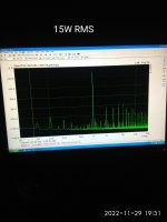
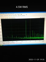
Power supply=+/-45v
Inp signal=560mV
Out =25 volt RMS 78W/8ohm
Attachments

Last edited:
- Home
- Amplifiers
- Solid State
- My MOSFET amplifier designed for music