dear sir,
why transistors become heated and destroy when input of an amplifier is not shorted?
That could be a sign of instability (wiring/layout etc). Its not an inherent issue to this design.
Blown amp due to open input is most often due to RF oscillation.
I came across this thread only now. The circuit in post 1 appears to be a typical single ended input stage with CFB with buffered VAS and CFP output stage. Should probably come out nice if the CFP stage doesn't give problems.
Interesting circuit. 60's input stage slowly moving on to an 80's or 90's output stage with refinements like CCS VAS load and dc servo control.
Has this been built yet ? Would like to know how it sounds.
I've tried a similar input stage with Darlington VAS and standard bootstrapped resistive VAS load and quasi comp MOSFET output stage. Sounds nice. Your amp has several refinements and a completely different output stage. Sounds promising. From what we hear , lots of people like the sound of amps with a CFP output stage ( eg. P3A).
Cheers.
Last edited:
A quick answer is that the amplifier is generating RF ( radio frequency ) signals on it's own without any input. Some parts cannot handle such signals and heat up very quickly and break down. Sometimes very dramatically !
An in depth explanation is not possible through a forum. You will need to read a good book on electronics. Your question is not silly but a proper explanation requires you to read a book on electronics. I think a short answer here will not do justice to the subject.
You can start here:
Parasitic oscillation - Wikipedia, the free encyclopedia
And from " High Performance Audio Amplifiers"
http://books.google.co.in/books?id=...=rf oscillation in an audio amplifier&f=false
Thanks ashok ") Yes its been built and been in daily use since around 2005.
Yes its been built and been in daily use since around 2005.
Starting post #283.
http://www.diyaudio.com/forums/solid-state/96192-post-your-solid-state-pics-here-15.html#post1417411
How does it sound... its all in the thread... check out some of the links in the first post.
Yes its been built and been in daily use since around 2005.Starting post #283.
http://www.diyaudio.com/forums/solid-state/96192-post-your-solid-state-pics-here-15.html#post1417411
How does it sound... its all in the thread... check out some of the links in the first post.
Hi Mooly,
I used a current source on the input transistor thereby negating the current flow through the main NFB resistor and made it very low in value.
I don't remember exact details now but when we did rigorous calculation of gain with NFB ( while studying !), simplification was valid only if NFB parts were much smaller than circuit elements.
In an unrelated circuit I used a resistive load with bootstrap and found it sounded better than a CCS in the VAS stage. Simulation showed lower distortion with CCS but a listening test showed otherwise.
So I used a resistive load with bootstrap in my version. Maybe it will sound better with a CFP stage which I had looked at but discarded because of the difficulty in getting N/P channel FET's easily. However it does sound very nice but there are better amps !
Filtering the input stage supply has become a standard. Ever since I heard the difference in an amp I made long ago. It was like chalk and cheese !
Never skipped that ever since. Regulated supply for the stages up to VAS is best especially if you can have an extra winding on the trafo or you use a voltage multiplier and regulator!
Note that some amps can sound great even without all this !
Cheers.
Last edited:
I agree there is no substitute for listening, because ultimately it is that "sense" that has to be satisfied. Using higher voltage and filtered rails for the front end and VAS is definitely one technique that would bring benefits. This type of amp has a somewhat "average" PSRR as it stands, although in practice its never an audible problem, hum and noise being inaudible.
Interesting to hear your observations on the CCS vs more traditional methods...
I'm currently working on a successor to this design, and its evolutionary rather than revolutionary, but it does promise to take things up a notch, addressing most of the compromises of the present design. That said, this is an amp that has stood the test of time.
Help required
Hi Mooly, this was indeed a great thread and the discussions i am sure will be very much beneficial for a great working build. The pcbs made by Alex are wonderful. I am very much keen towards building this amp. Just require few inputs.
1. Can we use 3 watts resistor in place of 5 watts...will it create any issue. With the existing supply.
2. The ground of the speaker to be taken from amps star earth...and the signal earth also Connected to same star earth ...am i correct?
3. Can 2 similar boards be bridged at the same input voltage , with the help of a external opamp ckt. Then Will any design considerations to be taken in to account. Or the design remains the same? The output will be floating...
4. What is the best transformer rating...I mean the otimum VA. keeping excellent performance and cost to min.
Waiting for your reply ....thanks in advance...regards Saraswat.
Hi, great to hear your thinking of having a go
1) Yes, 3 watts is OK for 8 ohm loading and the existing supply.
2) Speaker ground should return back directly to the PSU. The input grounds of both channels return separately back to the star ground.
3) Not really suitable for bridged operation. I certainly wouldn't recommend it.
4) A 300va transformer is ideal for a stereo pair.
An externally hosted image should be here but it was not working when we last tested it.
An externally hosted image should be here but it was not working when we last tested it.
Hi mooly, hw r u?...pls check my pcbs. And give your views.....about to complete the same
The FETs are yet to be populated...have ordered them and they r on the way...just cantcan't wait to hear them play..have read about the fake FET s. Just wondering the ones i have ordered are genuine or not.
If you have any methods to test them easily for genuine pls do post the same...waiting for your reply ...regards ...
That's looking good There is no easy way to test the FETs without actually putting them into a test circuit although a big giveaway would be if the Drain and Source pinouts were reversed making them like ordinary vertical FETs. So you could read across the inbuilt diodes across D-S to check that. Also if they needed a much higher gate-source voltage to turn on (meaning they could be ordinary vertical FETs).
You can actually test the board without the FET's fitted. If you apply power the speaker output should settle to essentially 0.00 volts DC give or take a few millivolts at most. Make sure the bias pot is on minimum resistance. And no load of course apart from the zobel network.
Nice work
There is no easy way to test the FETs without actually putting them into a test circuit although a big giveaway would be if the Drain and Source pinouts were reversed making them like ordinary vertical FETs. So you could read across the inbuilt diodes across D-S to check that. Also if they needed a much higher gate-source voltage to turn on (meaning they could be ordinary vertical FETs). You can actually test the board without the FET's fitted. If you apply power the speaker output should settle to essentially 0.00 volts DC give or take a few millivolts at most. Make sure the bias pot is on minimum resistance. And no load of course apart from the zobel network.
Nice work
Attachments
Hi Karl, just powered up the circuit without the FETs in place.
As per your instructions in thread 12 . Have checked the same step by step
Pls find the readings below.
Test Power Supply voltage 19.5 V.
Bias Pot has been kept at zero resistance between collectors.
The voltage across 100R. R5 is 8.65v
The voltage across pin 4 and 7 of opamp is 5.6v
The voltage across R17 and R22 is 11.69v each approx. ( which is higher , normal being 7 to 8 volt)
The o/p voltage is 0.26v
The issue is that Q4 and Q5 are slowly getting very very hot after 4 to 5 seconds of power on and have to switch off the power immediately..the degree of hotness gets worst when the bias pot resitance is increased....pls suggest. Have checked the boards for errors but both the boards are showing the same behaviour when powered....regards SS.
Last edited:
Hi,
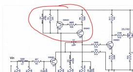
You have a problem with constant current circuit Q2 and Q3. It can only be a problem with either of the transistors or a board error.
How it works... Q3 is turned on via R6 (the 100k). Q2 has its base and emitter junction effectively across the 100 ohm. When the voltage across the 100 ohm rises above 0.6 volts Q2 turns on and limits the current flow in the 100 ohm by pulling the base of Q3 toward the emitter (the positive rail) turning it off.
The problem at this point can only be related to Q2 and Q3. Check for correct pin outs and polarity and make sure the transistors are PNP and of the correct type.
Attachments
Last edited:
Read the edit should have read at this point can only be related to Q2 and Q3
Fixing the current source is the first step. No matter what other problem there may or may not be, if the current source is OK there will never be more than around 0.7 volts across the 100 ohm.
Are you sure your transistors are from a reputable source ?
should have read at this point can only be related to Q2 and Q3Fixing the current source is the first step. No matter what other problem there may or may not be, if the current source is OK there will never be more than around 0.7 volts across the 100 ohm.
Are you sure your transistors are from a reputable source ?
Hi, Have fixed the current source and the voltage across. 100R is now 0.8v approx.
But the heating problem of Q4 and Q5 still persists. As already mentioned in above post.
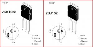
When the pot is turned clockwise the Q4 gets heated and it can't be touched and vice versa with Q5when pot turned to min position anticlockwise. Have checked the transistors they are genuine...pls suggest.
But the heating problem of Q4 and Q5 still persists. As already mentioned in above post.
When the pot is turned clockwise the Q4 gets heated and it can't be touched and vice versa with Q5when pot turned to min position anticlockwise. Have checked the transistors they are genuine...pls suggest.
Good to hear you fixed one problem. What was actually wrong out of interest ? Knowing that might help with other problems.
Q4 and Q5... again I suspect you have a problem in either construction or the parts. There is a low impedance path through Q4 (from its grounded collector) and then through the Q5 base and emitter junction to the negative rail. Are you sure Q4 and Q5 are OK ? The constant current problem could have overloaded and damaged them.
If you lift one end of R3 (4k7 at the input) then all the transistors should be off and nothing should get hot. That's a rough and ready check on whats going on. It might be worth doing.
Is the opamp a TL071 ? because that does provide the biasing for the input stage.
Who is didik?
I have no idea. There is a didik but he has never posted.
- Home
- Amplifiers
- Solid State
- My MOSFET amplifier designed for music