I explain the true significance of PM & GM in post #412 of tpc-vs-tmc-vs-pure-cherry ... PM, GM & Nyquist are also affected by loads. You need to look at what happens when you have different loads ...
Thanks kgrlee for the great explanations, your post there explained it in much simpler way than anywhere else I've seen, and your points about loads well taken.
Your discussions with David are very educating
") ... and it's funny that I'm reading stuffs about complex plane, Fourier transform, Laplace transform etc. these days, stuffs that I tried to avoid back in college days decades ago.
... and it's funny that I'm reading stuffs about complex plane, Fourier transform, Laplace transform etc. these days, stuffs that I tried to avoid back in college days decades ago.
Last edited:
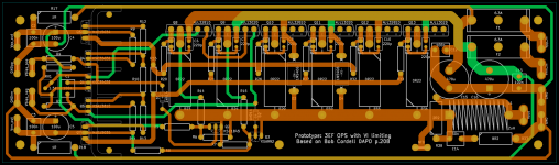
Please comment on this OPS layout
Having spent some more time reading and simulating, I think it’s about time to start some prototyping and testing, and cautious of the warnings I received about the VAS, I decided to first build the OPS in a separate board, so that I will have some flexibility on the IPS/VAS later. As my vero-board skill is very poor and printing PCB is pretty cheap (USD40 for 5 pieces of the below OPS board including shipping), I’ll go straight to print PCB for prototyping purpose.
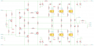
Attached is the OPS schematic and draft PCB layout of the prototype OPS board:
Having spent some more time reading and simulating, I think it’s about time to start some prototyping and testing, and cautious of the warnings I received about the VAS, I decided to first build the OPS in a separate board, so that I will have some flexibility on the IPS/VAS later. As my vero-board skill is very poor and printing PCB is pretty cheap (USD40 for 5 pieces of the below OPS board including shipping), I’ll go straight to print PCB for prototyping purpose.
Attached is the OPS schematic and draft PCB layout of the prototype OPS board:
- Board size is 238 x 69 mm
- Initially I tried to make it single sided, but with the onboard VI limiter and ThermalTrak diodes, it’s too difficult for me so I ended up using both sides.
- I put the main V+ and V- rail on top of each other to try minimizing loop area of the quiescent current
- Not sure if it’s a good idea, I route separate V+/GND and V-/GND to the lower power (left) section of the board, again on top of each other
- The bias spreader, pre-driver and driver transistors are mounted onto the same onboard heatsink for thermal compensation
- Track widths are from a minimum of 50 mil to a maximum of 200 mil
- The pad and hole sizes are slightly bigger than the standard ones, to make it easier for de-soldering just in case.
Attachments
Having spent some more time reading and simulating, I think it’s about time to start some prototyping and testing, and cautious of the warnings I received about the VAS, I decided to first build the OPS in a separate board, so that I will have some flexibility on the IPS/VAS later. As my vero-board skill is very poor and printing PCB is pretty cheap (USD40 for 5 pieces of the below OPS board including shipping), I’ll go straight to print PCB for prototyping purpose.
Attached is the OPS schematic and draft PCB layout of the prototype OPS board:
I would like to receive some remarks/comments about the layout.
- Board size is 238 x 69 mm
- Initially I tried to make it single sided, but with the onboard VI limiter and ThermalTrak diodes, it’s too difficult for me so I ended up using both sides.
- I put the main V+ and V- rail on top of each other to try minimizing loop area of the quiescent current
- Not sure if it’s a good idea, I route separate V+/GND and V-/GND to the lower power (left) section of the board, again on top of each other
- The bias spreader, pre-driver and driver transistors are mounted onto the same onboard heatsink for thermal compensation
- Track widths are from a minimum of 50 mil to a maximum of 200 mil
- The pad and hole sizes are slightly bigger than the standard ones, to make it easier for de-soldering just in case.
I will not comment the layout, because I think tha use of separate PCBs for IPS and OPS is not so good idea.
Just small suggestion. The bias multiplier factor for TT diodes tempco is too high. From my experience R3 should have higher value, otherwise the amp is going to be to much thermally overcompensated. Ratio R1/R3 +1 defines the multiplication factor for TT diodes tempco.
It is pity not to put to good use not used TT diodes, here is very good explanation The YAP Output Stage.
Your EF3 is fast-slow-slow; I think in this case you should put the zobels around the drivers' base-collector pins instead of the output devices.
You might consider KSA1220/KSC2690 for your predrivers. Both sexes are available in the high gain "Y" grade unlike the KSA1381/KSC3503, which are more suitable as a VAS transistor IMHO. Any old cheap BD139 for the bias generator.
The output devices are virtually on top of each other and you should consider spacing them out a little more to aid assembly.
Try to move the power pins and main decouplers in between the two triplets; lose the fuse holders if necessary and relocate them to the PSU board. Increase the track width of the main rails and speaker out track. Move the output coil and ancillary parts left and take a T at the midpoint. You will gain a little space which can be used to space the outputs slightly and shorten the board.
Your IV protection component values will take quite a bit of adjusting to get protection while still allowing all valid audio signals to pass to all valid audio loads.
You can do much of this by simulation to show what ballpark values are required.
But semiconductor "turn on" voltages are very dependent on Tj. This can only be determined in the working prototype after you know what to look for. In the meantime omitting the two diodes to turn off the IV might get the amp working without unintended intervention of the IV.
Your IV has a DC triggering value and a DC limiting value.
You have made no provision to for short term transient capability of the output stage.
The IV should allow short term transient currents up to around 20times the permissible DC values to pass through to the valid load.
The two protection transistors can benefit from coupling to the hottest part of the amplifier. This reduces the trigger levels as the amplifier heats up.
Last edited:
... From my experience R3 should have higher value, otherwise the amp is going to be to much thermally overcompensated. Ratio R1/R3 +1 defines the multiplication factor for TT diodes tempco.
It is pity not to put to good use not used TT diodes, here is very good explanation The YAP Output Stage.
Thanks Dadod for your suggestions, I'll increase R3 to 6.8k then, to give (2.2/6.8+1)*3.4 = 4.5mV/degC. I also thought about making some use of the remaining TT diodes, but routing them to the left side of the PCB is a challenge (without using vias, something I don't really want to), I'll read the link and think again.
Your EF3 is fast-slow-slow; I think in this case you should put the zobels around the drivers' base-collector pins instead of the output devices.
Thanks Ranchu32, I've seen people using different ways to stabilize a EF3, but I'm lacking some basic electronics knowledge to understand the mechanism behind, could you elaborate further, or point me to some relevant resources. (I'm reading D.Feucht's book to try to learn some basics, but to work through all those algebra will take me a year to finish the 4 volumes.)
You might consider KSA1220/KSC2690 for your predrivers. Both sexes are available in the high gain "Y" grade unlike the KSA1381/KSC3503, which are more suitable as a VAS transistor IMHO. Any old cheap BD139 for the bias generator.
Thanks for the transistor recommendations, but I already have a stash of E-grade KSA1381/KSC3503 so I'll simply use them, especially since it took me some effort to get genuine E-grade KSC3503. One thing that borders me slightly is that despite having 60 pieces of each, I can't find one single pair which are hfe matched (all 3503 have hfe closely around 165, and all 1381 closely around 132)
... Move the output coil and ancillary parts left and take a T at the midpoint. You will gain a little space which can be used to space the outputs slightly and shorten the board ...
Good suggestion, I'll try.
... Your IV protection component values will take quite a bit of adjusting to get protection while still allowing all valid audio signals to pass to all valid audio loads.
You can do much of this by simulation to show what ballpark values are required.
...
Thanks Andrew for your comments, could you elaborate your remarks on the VI component values.
The current values are computed so that with 1 output pair, it can handle any kind of reactive load at 10 ohm, at the same time always within the 1 sec SOA. With 3 output pairs, in theory it can handle any kind of reactive load at 3.34 ohm or above and never activates. Simulations so far also suggest the VI limiter is working as expected.
If you haven't already, I would strongly suggest you read Michael Kiwanuka's article on transparent VI limiting, featured on Bonsai's site.
Thanks, very useful article and I haven't read it before. By a quick look, the VI limiter I used is very similar to fig.1 of the article, but without the shunt capacitors. I'm aware of more sophisticated limiters from other sources, but I tried to keep it simple so just chose the most basic one (and the amp is probably already too complex for a newbie like me
)Firstly, if you are buying PCBs, these days, double layers are as cheap as single and plated through holes are essentially free.
Like your power rails on top of each other.
I would try & move your output rail as far up as possible to be closer to the power rails. It's not the quiescent current loop that you have to worry about but the yucky Class B currents at full power. The current flows from PSU, via your nice 'twisted wire' PSU rails, the O/P devices and then your output rail to the speakers then back to the PSU. Its this loop that needs to be as small as possible.
I won't comment on the triples which I don't like but suggest you look at Toni's 2stageef-high-performance-class-ab-power-amp-200w8r-400w4r for what is probably the best, most complete & tested implementation of Self's Blameless. Good ideas on layout too though like Damir, I don't like separate driver & O/P boards.
Dunno about your earth rails but I'm wary about having them on either side of the PCB. Potential for a big loop aerial with loadsa yucky currents happening inside the loop .. but dunno how these connect to the sensitive i/p & f/b earths.
Lastly, Self observes that the back of plastic o/p devices can get very hot so it is useful to arrange for a heavy duty Aluminium clamp rather than individual mounting screws if the PCB layout allows this. Hot = low thermal resistance to the die.
Last edited:
If you look at Toni's thread, you'll note that he achieves 'real life' performance that practically none of da supa dupa triple circuits manage.kgrlee, what is it about triples that you don't like?
2stageef-high-performance-class-ab-power-amp-200w8r-400w4r
In my tpc-vs-tmc-vs-pure-cherry thread, I show how to achieve 1ppm THD20k @ 50W 8R with very simple circuits.
Simpler circuits are MUCH more likely to replicate SPICE world in 'real life'. You can have MUCH better layout, earthing & decoupling if you are versed in the art.
The YAP page lists some more problems with triples. I am not averse to complexity IF it brings some benefits. But if I can achieve what I want (in this case 1ppm THD20k) without complexity ....
The one triple caveat I haven't re-visited this Millenium is that some people claim that with ThermalTrak, a triple O/P stage will stabilize quickly. This was REALLY important to me in Jurassic times and triples were MUCH worse than EF2. It will take hands on experience on my part to be convinced.
IMHO, one of the most important parts of Self & Cordell is how they DESIGN for Thermal Stability. I have some 'real life' experience doing this but question some of their recommendations.
Obviously pushing EF2s also has its drawbacks - most of all, current gain of a double is somewhat limited. You must ensure that beta droop is minimized (and a good amount of beta and GBW is present to start with), and a buffered PP VAS with a good amount of "grunt" would eventually be preferable if you expect to be able to drive 4 ohm (or less) loads at high power levels. Which essentially boils down to better-quality parts being required, as well as higher Pdiss in the VAS. It's a plain ol' complexity - power - performance tradeoff again.
Back in the late '70s, Prof. Leach used a triple in spite of its potential drawbacks (higher complexity, more parasitics, lower thermal stability) because he had to work with the kind of power transistors that were available at the time. We may eventually get back there eventually as good driver and VAS transistors die out (they tend to have come from the high-voltage video department, and we all know how popular CRTs are these days), though hopefully the demand from the audio crowd will be sufficient to keep some of them in production.
Back in the late '70s, Prof. Leach used a triple in spite of its potential drawbacks (higher complexity, more parasitics, lower thermal stability) because he had to work with the kind of power transistors that were available at the time. We may eventually get back there eventually as good driver and VAS transistors die out (they tend to have come from the high-voltage video department, and we all know how popular CRTs are these days), though hopefully the demand from the audio crowd will be sufficient to keep some of them in production.
I would have expected the triple to give much improved VAS gain, hence OLG, due to the much higher Zout.
If you plot the loop gain of a simple Blameless with enhanced VAS & EF2 without compensation, you find a stupendous amount of gain.
If you could use more of this gain safely without stability problems, you would have 1ppm THD20k and other good stuff immediately.
Adding more gain with triples, fancy topologies bla bla doesn't give you more usable gain. It only makes it more difficult to use .. cos extra stages mean extra roll-offs, more stability problems, more disparity between SPICE world & 'real life' and other evil stuff. That's why very few such supa designs even equal the very simple design in my thread.
My preference is always the simplest possible circuit that equals or surpasses complicated supa dupa ones.Do you have a preferred topology? SE or PP VAS? Do you buffer the VAS at all hang the EF2 output stage directly off it?
This Millenium, I'm a real beach bum and am just amusing myself by seeing if LTspice can emulate a lot of 'real life' experience in da previous century.
There are 3 reasons why tpc-vs-tmc-vs-pure-cherry is based on a Blameless topology.
- it is the simplest topology for a given supa THD performance.
- I have a lot of Jurassic 'real life' experience with it
- Lastly, Toni's 2stageef-high-performance-class-ab-power-amp-200w8r-400w4r is a Blameless and he has been good enough to try some of my heretical ideas and give me 'real life' measurements to improve my sims. I'm fairly confident what I show will have 'real life' <10ppm THD20k and be stable.
A pseudo guru in that thread proposed a more complicated circuit using triples but his THD20k is some 20dB worse than my simple circuit and he has wonky stability too.
Many of these supa circuits run the VAS at even higher Pdiss than I do. If I used their VAS Pdiss, I could look at simplifying my stuff even further.
_______________
But Blameless isn't my favourite topology. It has the best THD/simplicity but also problems when overloaded though these can be alleviated with careful design as with Toni's excellent example.
My favourite topology is a simpler variant of Bob Cordell's push pull VAS using MOSFETs without evil HEC
But I dislike recommending stuff for which I haven't got at least some link to 'real life'.
Finally, after much poking, we have better-power-mosfet-models-ltspice
Now I only need to find someone with an AP or equivalent who is willing to make expensive stuff & test it on the recommendation of a beach bum.
Last edited:
... I would try & move your output rail as far up as possible to be closer to the power rails. It's not the quiescent current loop that you have to worry about but the yucky Class B currents at full power. The current flows from PSU, via your nice 'twisted wire' PSU rails, the O/P devices and then your output rail to the speakers then back to the PSU. Its this loop that needs to be as small as possible ...
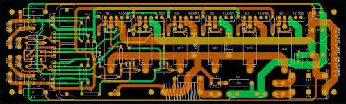
Thanks again kgrlee for your comments, very true indeed so I've moved the power rails closer to the output rails, as close as I possibly can. Attached is the revised version.
I also agree with you about achieving the results with least complexity, but this amplifier is "an exercise" for me to learn about amplifier, so a little more complexity than really needed could be fun also. True guru will seek for elegant simplicity, point taken (maybe one day I'll design a SIT based one transistor headphone amp
)Attachments
- Status
- This old topic is closed. If you want to reopen this topic, contact a moderator using the "Report Post" button.
- Home
- Amplifiers
- Solid State
- My First Amplifier Design