With the very helpful suggestions by mjona, the amplifier's issues have been greatly reduced. In fact, I am listening to music with this amplifier without problems. I will further improve the signal source's performance by replacing the switching power supply with a linear power supply. This will also eliminate the remaining very feeble hum issues which are due to insufficient filtering.
Thanks to all who helped. This thread can be now considered concluded and its aim fulfilled.
Thank You.
Thanks to all who helped. This thread can be now considered concluded and its aim fulfilled.
Thank You.
The following is Not a design question:
I am planning about testing this amplifier for a very very long period of time for stability and reliability. I am particularly aiming at determining whether the amplifier is SAFE enough to be used in a home environment where a fire can cause huge damages. Therefore, I am interested in whether internal termperature rise when the amplifier is unloaded but powered on for very long periods of time.
To achieve this, I will connect a 3A quick blow fuse in series with each speaker and a line 2A quick blow fuse to cut AC power in the event of a fault.
I am aiming to leave the amplifier on for several days, but without load. I will load it only intermittently.
Last edited:
I'm not so sure an extended soak test is the way to go for assessing fire risk... what you really need to be sure about is whether the enclosure could contain any likely hotspots or flaming components. Such events are usually short lived and the component/s burn out quickly while admittedly making a huge smell and lots of smoke. Mains switches and wiring and of course the transformer are other considerations. There should be fusing present to open the live feed in the event of a fault which I see you mention.
The following is Not a design question:
I am planning about testing this amplifier for a very very long period of time for stability and reliability. I am particularly aiming at determining whether the amplifier is SAFE enough to be used in a home environment where a fire can cause huge damages. Therefore, I am interested in whether internal termperature rise when the amplifier is unloaded but powered on for very long periods of time.
To achieve this, I will connect a 3A quick blow fuse in series with each speaker and a line 2A quick blow fuse to cut AC power in the event of a fault.
I am aiming to leave the amplifier on for several days, but without load. I will load it only intermittently.
You need an output dc protection circuit so if this swings to a rail voltage due to component failure resulting from elevated temperatures, the speaker coil does not overheat and set off a fire inside the speaker. If the equipment gets hot there are fuses that melt with temperature that are used for hairdryers that you could try or possibly a thermostat to disconnect the mains.
Temperature Rise Testing:
This post is NOT intended to ask for help, but to show readers that visiting diyaudio.com, can help them build a well performing amplifier. So, take this as a sincere Thank you, all.
Temperature Readings of heatsinks on NO load/audio signal:
At switch on, t = 0s:
VAS 1: 25C
VAS 2: 25C
Power Heatsink 1: 25C
Power Heatsink 2: 25C
At t = 11-14 minutes:
VAS 1: 32C
VAS 2: 32C
Power Heatsink 1: 27C
Power Heatsink 2: 28C
At t = 18-22 minutes:
VAS 1: 34C
VAS 2: 34C
Power Heatsink 1: 27C
Power Heatsink 2: 28C
Last edited:
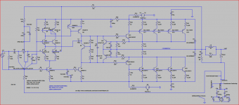
Further studying the remainder of the original PCB that holds the smoothing stage and the output stage, revealed rail fuses can be installed safely. These can be installed on the original PCB after cutting the thick rail tracks.
The original 20A slow blow fuse is to be removed and its place shorted with a 1mm square copper wire. This fuse is presently on the 0V common terminal.
Inspecting the original PCB, I also noticed the points from which power is supplied to the sensitive input stage, has a hum/buzz component added by the track segment's resistance. The reason is this particular track segment, has smoothing capacitor charging surges flowing in it. I will move these points to completely avoid these unwanted hum/buzz components.
Needless to state, all these procedures are very tedious to implement, and a lot of patience has to be exercised.
Adding rail fuses will let me test the amplifier for very long periods of time to establish its reliability.
Common Mode Rejection Ratio Calculaton:
The value for the RAW CMMR was found to be: 13700
In dB this value results in: 20*log(13700) = -82.7dB
Code:
Using the formula:  CMMR = (Re + Ze)/Zcs
Where:
Re = Emitter Resistance
Ze = Emitter AC Resistance
Zcs = AC resistance of the current source used by the input stage
The value for the RAW CMMR was found to be: 13700
In dB this value results in: 20*log(13700) = -82.7dB
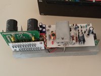
Since the issue of crackling sound has been re-encountered, I opened the amplifier box to do repairs to the amplifier modules. I am attaching a much better quality photograph of an amplifier circuit complete with its heatsinks.
DIY is hard, but it is fun and satisfying in the long term. The module illustrates clearly that DIY without special tools was a factor in its building.
Needless to state, to use this forum and build your own amplifier, you do not need to be some kind of genius: the help here is enough.
DIY is hard, but it is fun and satisfying in the long term. The module illustrates clearly that DIY without special tools was a factor in its building.
Needless to state, to use this forum and build your own amplifier, you do not need to be some kind of genius: the help here is enough.
Attachments
Having the innards of this amplifier dismantled I intend to do some more changes to the circuit according to advice given to be by mjona some over two years ago. These changes involve the value of the resistors feeding the bases of the driver stage. To tame the amplifier from aggressively clamping onto a rail, I had to add two resistors in series with the emitters of the driver transistors. These transistors already have their emitters sensing the current through a 0.1 Ohm resistance. The emittter resistor value is 3.3 Ohm. My intention is to increase the resistors' value feeding the driver bases in the hope of achieving DC stability that way.
Why is the amplifier clamping without the above mentioned resistors? My humble hypothesis.
The driver transistors' input characteristics have very sharp current increases for very small voltage changes. A resistor in series with their emitters componsates for this by stealing the extra voltage needed to cause these abnormal current increases. Needless to state, I could not simulate this behaviour notwithstanding I am using the same transistor numbers under LTSpice. My temptation is to change these two transistors with two with a better behaviour.
Having the innards of this amplifier dismantled I intend to do some more changes to the circuit according to advice given to be by mjona some over two years ago. These changes involve the value of the resistors feeding the bases of the driver stage. To tame the amplifier from aggressively clamping onto a rail, I had to add two resistors in series with the emitters of the driver transistors. These transistors already have their emitters sensing the current through a 0.1 Ohm resistance. The emittter resistor value is 3.3 Ohm. My intention is to increase the resistors' value feeding the driver bases in the hope of achieving DC stability that way.
Why is the amplifier clamping without the above mentioned resistors? My humble hypothesis.
The driver transistors' input characteristics have very sharp current increases for very small voltage changes. A resistor in series with their emitters componsates for this by stealing the extra voltage needed to cause these abnormal current increases. Needless to state, I could not simulate this behaviour notwithstanding I am using the same transistor numbers under LTSpice. My temptation is to change these two transistors with two with a better behaviour.
I think you have a wheel within a wheel with the larger feedback loop of the CFP with local nfb from your power transistor emitter resistors and these are somewhat out of phase. This situation is eased if your power transistor emitters have a direct connection to the supply rails and the ballast resistors for these are placed in the collector connections to the output line.
I have simulated the circuit with 3R3 in the driver transistor emitter connections. These will cause the collectors connected to the power transistor chains to move closer to the supply rails to the point where setting the output quiescent current becomes a problem. Reducing this to 2R2 makes some small improvement. I looked at the Vbe section but didn't spend a lot of time with this as my wife has care needs.
I have attached a couple of simulations you might be able to make use of. THD is a little better with the xyz circuit.
Attachments
I had some input around post 190 where I talked about a lower power version. In this like you I omitted Q5 which gives rise to an anomaly at low frequencies in a Tian plot - this has some waviness at the top where it should be a straight line. If Q5 starts to limit the collector current in Q4 in normal rather than fault conditions the result will be sampled by the 100pF nfb capacitor. Q4 is already protected by a base stopper resistor and the added components to include Q5 seem to be an over complication.
Attachments
Last edited:
To mjona: Thanks for taking the time to reply. It is important that I understand why the introduction of the two 3.3R driver emitter resistors make achieving a bias a difficult task. I experienced this in practive when I was setting the amplifier up and had to use these resistors. When I have time, hopefully tomorrow, I will look again at the thread to try to understand why these resistors cause trouble: I would like to remove them but the two driver transistors seem to have different transfer ratios (betas). This may cause one half of the amplifier to clamp because of the extra unbalanced gain.
If I am wrong, please correct me. I will not be offended.
Thanks.
If I am wrong, please correct me. I will not be offended.
Thanks.
Your output transistors have emitter resistors which will have some limiting effect on current due to nfb signals across each of these resistors. You have the same situation with the 3R3 driver transistor. I found with this arrangement it was not possible to set the output stage standing current. At an inconvenient point no change to the trim adjustment made any difference. Moving the power transistor emitter resistors so these were in series with the collectors made all the difference. The 3R3 emitter for the drivers is still there.To mjona: Thanks for taking the time to reply. It is important that I understand why the introduction of the two 3.3R driver emitter resistors make achieving a bias a difficult task. I experienced this in practive when I was setting the amplifier up and had to use these resistors. When I have time, hopefully tomorrow, I will look again at the thread to try to understand why these resistors cause trouble: I would like to remove them but the two driver transistors seem to have different transfer ratios (betas). This may cause one half of the amplifier to clamp because of the extra unbalanced gain.
If I am wrong, please correct me. I will not be offended.
Thanks.
A stripped down version of the circuit minus all short circuit elements is attached. If you like the emitter resistors in the output transistors there could be other ways to deal with the situation like increasing the values of R20 and R22 to increase the voltage drop across the base emitter junctions of the output power banks.
Attachments
Last edited:
Well that last suggestion should work. One point I forgot to mention is that decreasing the closed loop gain reduces THD. You can use an IC op.amp to make up for the loss of gain and since this would occupy a smaller area than your power amplifier does the whole will less sensitive to picking up radiated fields and have lower noise in general.
The answer
See post 85 on page 5 second paragraph.edbarx
and why did you choose the option of collectors to the output, and not the usual one (emitters)? Does it sound better this way or for some other reasons?
- Home
- Amplifiers
- Solid State
- My attempts at a design of a 3 stage amplifier