Hi Fab!
Yes, I am also not perfectly lucky with that proposal.
And even worse, I would have prefered less gain in this stage (i.e. 22k and 22k),
but you already pointed out that the lower MosFet needs a Vgs bias of some single volts in order to get a suitable idle current....
So I simply proposed a low value for the emitter resistor.
And even with this you are still right, if we assume Vgs=4V then there will be around 1.6mA in the 22k resistor and also in the 1k emitter resistor.
Means Vce of the bjt would be around 2.3 V.
Low voltage, but still somehow operative....
I did not propose to run this without emitter resistor because of gain matching in the upper and lower side.....
Cheers Markus
uhps, typing error:
my preferred ratio of collectro resistor to emitter resistor would be around 5. Some gain is needed as the op amps cannot slew up to 40V, but the upper MosFet need a drive with full swinging capability.
I think, already the fact that the emitter of the upper BJT is connected to ground would cause trouble, because this will not allow much negative swing at the output.....
...puh...., I am glad that I do not really need to get this beast running in a proper way!
hi fab
be sure I am
and I do realy appreciate all your comments
and ChocoHolic's and by all of you...
but
if you,d like to do me a favour look once more on my worthless schematic and ensure me that the feedback is positive
I don't get this point
well i'm a beginner, though...
looking forward to seeing your answer
darkfenriz said:hi fab
be sure I am
and I do realy appreciate all your comments
and ChocoHolic's and by all of you...
but
if you,d like to do me a favour look once more on my worthless schematic and ensure me that the feedback is positive
I don't get this point
well i'm a beginner, though...
looking forward to seeing your answer
Hi darkfenriz
Yes I confirm what ChocoHolic has noticed, it is a positive feedback thus it is not possible that it could work.
For example, take the upper "positive" signal path where the first opamp does not invert the signal but the second one does. The following NPN transistor is an emitter follower and the N mosfet also in an emitter follower too that let the signal inverted which forms part of the ouput signal that is fed back to the "-" of the first opamp. So, for the first op-amp, it tries to compute the input signal by subtracting a portion of the "inverted" ouput signal: thus (-)(-) = (+) which is positive.
I hope it is more clear even though it is not that simple to explain here.
Fab
Hi fab!
Yes, I can't add much to your explanation.
...can only try to find other words for the same thing...
Hi dark!
...let's follow the signal path.
If we move the inv input of the first OP upwards, then the output of this first OP moves down. Now an inverting amp is following. Behind this the signal will move up . Also behind the upper BJT the signal will move upwards and also behind the Mosfet.
So if the inv input of the first OP is pulled upwards, then also your output will move upwards. Overall the signal is not inverted anymore.
Bye
Markus
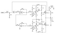
hi darkfenriz
The feedback polarity problem is now solved.
However, other problems may need to be addressed.
For example:
- the DC polarisation of the mosfet seems extremely high for the positive signal path and also probably too high for the negative one (check data sheet VGSoff voltage).
- the DC polarisation of the BJTs is also to review.
- the opamps "see" a DC load of 2k ohms with with 20V (40V/2) if it tries to adjust the DC to 0 V. This makes 10 ma which is too much for most opamps.
- what is the purpose of the 1uf cap at base of BJTs?
- you should also consider to increase the maximum possible output swing of the BJT (Vce) since the upper mosfet has a unity gain (follower).
Check previous posts again.
Good luck
Fab
...yes, the gate drive voltage of the upper Mos is excessive and will pull up the output to a high positive DC value.
Also the lower MosFet is adjusted to an gate source voltage around
7V, did you check how much bias current this will cause if you use an IRF 710? !!
Please also note that the DC forward gain is zero in that new schematic. So the feedback and the OP amps will not be able to regulate the DC offset to a reasonable value. DC offset is now defined by MosFet biasing only.....
Furtheron the OP amps outputs might now stick to positive or negative rails, because the first OP amp has no closed DC feedback loop anymore.....
Do you use the 1uF caps at the base of the BJTs for frequency compensation? They form a pole at 111Hz.
If you need audio suitable OP amps which can handle high output currents (refer to fabs posting), then I would recommend the cheap and old (but still not bad) NE5534. It is designed for 600Ohm load at full swing, which means +/-12V (supply +/-15V) into 600 Ohms
==> up to around 20mA is acceptable....
Bye
Markus
P.S.
...you are going for a very tough path of learning, if you really want to make this design running...
- Status
- This old topic is closed. If you want to reopen this topic, contact a moderator using the "Report Post" button.
- Home
- Amplifiers
- Solid State
- mosfet and opamp amplifier