"The paradox of simplicity is that making things simpler is hard work!"
--- Bill Jensen
https://www.amazon.com/gp/product/0...de=as2&tag=disrupt-20&linkId=TL3ZSXSEY3KDFDIX
-RNM
--- Bill Jensen
https://www.amazon.com/gp/product/0...de=as2&tag=disrupt-20&linkId=TL3ZSXSEY3KDFDIX
-RNM
Last edited:
That looks very good. Have you loaded and tested it -- measurement or listening?
THx-RNMarsh
For now exist only on drawing board, sorry.
When I finish making layout, I can post gerber, I am kind of slow with soldering
 .
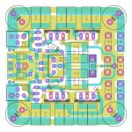
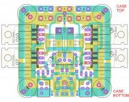
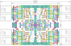
.Regarding layout, please comment if there is something needs changing/improving?
BR Nenad
Regarding layout, please comment if there is something needs changing/improving?
BR Nenad
just make sure to allow for some heat sinking of the output transistors --
just make sure to allow for some heat sinking of the output transistors --
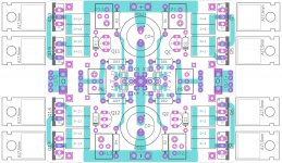
Output transistors will be mounted beneath the PCB.
Two mount options in my POW:
1. Yours
, fixing to the bottom of the case2. Mini power amp like case with lateral heatsinks, for example:
Douk Audio Amplifier Chassis General Aluminum Shell Pre-Amp Enclosure DIY Box | eBay
internal lateral height needed is 50 mm
With heatsink like this, I believe much higher bias is possible.
Attachments
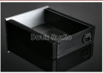
That's the same case I used for a pass F5 headphone amp...It's called the "2107 chassis" on eBay, etc.
It is way, way more than enough. Even with 300ma bias. Probably more.
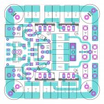
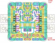
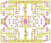
Can we find a way to put a hole in the pcb for the output BJT mounting screws when they are mounted on the bottom of a chassis or on heatsinks?
It is way, way more than enough. Even with 300ma bias. Probably more.
Can we find a way to put a hole in the pcb for the output BJT mounting screws when they are mounted on the bottom of a chassis or on heatsinks?
Attachments
Can we find a way to put a hole in the pcb for the output BJT mounting screws when they are mounted on the bottom of a chassis or on heatsinks?
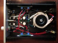
One picture is worth thousend words
PS Power&Output connectors are spade ready
Attachments
Jack has matched devices to sell.I like it a lot. Anybody have a source for matched jfets?
If all bets are off, let me know. I can match a couple pairs from my Fairchild 2N5457's and 2N5460's.
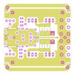
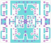
pads
Hi,
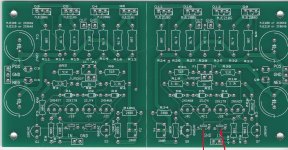
I bought this PCB about two years ago, but I didn't get any schematic with it.
That wouldn't be a big deal because all the component values are printed on the board. Except I can't find any explanation for the pads called J1 to J4. They look like SOT23 footprints ,which doesn't tell me to much. So I ask here if somebody could explain the purpose of these pads? Thanks.
Hi,
I bought this PCB about two years ago, but I didn't get any schematic with it.
That wouldn't be a big deal because all the component values are printed on the board. Except I can't find any explanation for the pads called J1 to J4. They look like SOT23 footprints ,which doesn't tell me to much. So I ask here if somebody could explain the purpose of these pads? Thanks.
Attachments
Hi,
I bought this PCB about two years ago, but I didn't get any schematic with it.
That wouldn't be a big deal because all the component values are printed on the board. Except I can't find any explanation for the pads called J1 to J4. They look like SOT23 footprints ,which doesn't tell me to much. So I ask here if somebody could explain the purpose of these pads? Thanks.
I have the same board and kit from Jack. J1 to J4 are surface mount alternatives for the 2N5457 and 2N5460 jfets which are getting harder to get in their TO-92 package(in position J1C - J4C). The surface mount part numbers are MMBF5457 and MMBF5460.
Since this is a published design, you should purchase a print of the article from Linear Audio(https://linearaudio.net/article-detail/2118), which has the schematic and BOM etc. If it is a Rev 2 board, Jack has made provision for a trimmer pot(P2/P4) that may not be mentioned in the original article. I can send you a scan of the package that Jack sent me if you PM me.
Hi,
I bought this PCB about two years ago, but I didn't get any schematic with it.
That wouldn't be a big deal because all the component values are printed on the board. Except I can't find any explanation for the pads called J1 to J4. They look like SOT23 footprints ,which doesn't tell me to much. So I ask here if somebody could explain the purpose of these pads? Thanks.
PM me
this is the second version of the boards -- it's set up so that you can use the transistors Dick had in his original article, the Toshiba's or SMT devices which are still in current production.
the board also incorporates a suggestion by Dick to allow adjustment of the bias. that's why there are two potentiometers.
- Home
- Amplifiers
- Headphone Systems
- Marsh headphone amp from Linear Audio