What grade are the jfets? Check the schematic in post #66, the idss rating is written in near the jfet.
If V grade, a pair per channel is necessary, if bl grade, you must use two pairs per channel to get the idss value high enough.
Juma, what happens in the circuit if we use just in bl grade jfet, say idss 8-10mA without changing any other value?
If V grade, a pair per channel is necessary, if bl grade, you must use two pairs per channel to get the idss value high enough.
Juma, what happens in the circuit if we use just in bl grade jfet, say idss 8-10mA without changing any other value?
... particular type of matching...
It's best to match them at the Id they'll be working at in the real circuit, i.e. with 10R degeneration, or at Idss if you mean to run them at Vgs=0 as in Mr. Pass' version from presentation.
Any point in playing with different Rdeg for the K170 and the J74 in this circuit to achieve perfect complemetarity?It's best to match them at the Id they'll be working at in the real circuit, i.e. with 10R degeneration, or at Idss if you mean to run them at Vgs=0 as in Mr. Pass' version from presentation.
Any point in playing with different Rdeg for the K170 and the J74 in this circuit to achieve perfect complemetarity?
That's why there is a 20R pot between their sources. Some time ago EUVL wrote in other threads about achieving better complementarity of k170/j74 - maybe you should search for his writings.
And yes, as tinitus mentioned, in my first test-build I used BL grade k170/j74 (Idss of about 8mA).
It's beneficial to use higher Idss parts because higher output level means higher current swing through JFETs but, as usual, compromises are at play: higher Id at higher Vds brings higher Pd; using higher source-to-GND resistor and higher output I-to-V resistor allows for smaller current swing i.e. better linearity but it raises the distortion at higher frequencies (because of parasitic capacitance) and introduces the need for output buffer.
It all boils down to what one wants from this circuit: up to 10V_peak at the output and up to 12dB gain it's all very easy...
Juma,
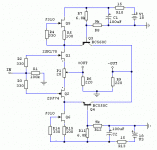
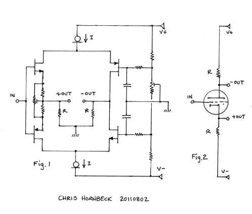
I am interested in using the unity gain version of the LSK circuit as a phase splitter for bridging amps. I mean the schematic which you posted in F4 amp thread (post 3942), also attached here. Re: this schematic:
Q1: The output impedance here is 220 Ohm, right? and
Q2: what grade (Idss) are 170/74 pair? Can I use BL grade parts (Idss~7mA) and if yes how do I adjust the current sources and other values? Thanks a lot. (p.s. if the Zout after changes gets higher, I can always run both Out+ and Out- signal, each through a separate buffer, right?
Thanks a lot!
Attachments
koja,
q1:around that value yes.
q2:higher idss the better if i m not mistaken. pot along jfet ccs source resistor to adjust,if the jfet are not matched. r6 r9 are a round the actual value of output impedance. you can use separate buffer if you want regardless.
please correct me if i m wrong , someone
edit: hmm...maybe output impedance of + phase is lower...
Last edited:
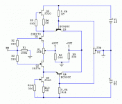
Yes, but only on the -OUT. On the +OUT it's about 20-30 Ohms. So there is a difference in Zout value between the outputs but it won't matter if the load (next stage's Zin) is high enough (10k or more).Q1: The output impedance here is 220 Ohm, right?
For that phase splitter I used BL parts (~8mA Idss) so your JFETs will be fine.Q2: what grade (Idss) are 170/74 pair? Can I use BL grade parts (Idss~7mA) ...
Look at the sch. in attachment, I think it will serve you a bit better. CCSs (Q5, Q6) should be set for 15-17mA each at 5V (both should deliver the same current) before you put them in the circuit. Value of R4, R10 will set the current through Q5,Q6. Start with the given value and see where it'll take you. P2 sets the DC offset at -OUT (like in Chris Hornbeck's original schematic)...how do I adjust the current sources and other values? ...
Now it's 330 Ohms at -OUT (it sounds better to me that way, you can try different values) and it still doesn't need a buffer to drive any standard amp (Zin of 10k or more) but yes, you can add buffers on both outputs if you plan to drive extra long cables and/or unusual loads (F3, TVC, or similar)....if the Zout after changes gets higher, I can always run both Out+ and Out- signal, each through a separate buffer, right?
Attachments
Works great. Hard to beat in terms of simplicity/parts count versus sound qualityà la CEN")

Yes, but only on the -OUT. On the +OUT it's about 20-30 Ohms. So there is a difference in Zout value between the outputs but it won't matter if the load (next stage's Zin) is high enough (10k or more).
For that phase splitter I used BL parts (~8mA Idss) so your JFETs will be fine.
Look at the sch. in attachment, I think it will serve you a bit better. CCSs (Q5, Q6) should be set for 15-17mA each at 5V (both should deliver the same current) before you put them in the circuit. Value of R4, R10 will set the current through Q5,Q6. Start with the given value and see where it'll take you. P2 sets the DC offset at -OUT (like in Chris Hornbeck's original schematic)
Now it's 330 Ohms at -OUT (it sounds better to me that way, you can try different values) and it still doesn't need a buffer to drive any standard amp (Zin of 10k or more) but yes, you can add buffers on both outputs if you plan to drive extra long cables and/or unusual loads (F3, TVC, or similar).
Thanks Juma for a new proposal. Is it possible to use +/-33V that already exist in PS?
Of course - everything stays the same except the value of the output I/V resistor and P2 which is introduced to enable separate DC offset setting for -OUT (P1 does it for +OUT)....Is it possible to use +/-33V that already exist in PS?
Of course - everything stays the same except the value of the output I/V resistor and P2 which is introduced to enable separate DC offset setting for -OUT (P1 does it for +OUT).
Excellent, any suggestion for I/V resistor value in case that 2SK170V/2SJ74V or 2Sk246/2SJ103 pair will be used?

Look at the schematics. With k246/j103 you can use somewhat higher values since they have lower parasitic capacitance. It's a compromise - higher resistor values give better general linearity (smaller current swing is needed) but they tend to narrow the band and increase the Zout.Excellent, any suggestion for I/V resistor value in case that 2SK170V/2SJ74V or 2Sk246/2SJ103 pair will be used?
You can't relay on simulations here if you are not prepared to make models that reflect the real world parasitics. Listen to differences that various values produce and/or measure the results. When designing/measuring for bandwidth I aim for such a frequency response that provides zero phase change at 20kHz with realistic load (1-2m coax cable terminated with 10k||10p-1n).
Hi!
I would like to build the LSK-Pre to drive my F6 (buffered version).
Unfortunately I am not good in electronics, so I need your help.
I have got two matched pairs of K170/J74 BL with an Idss of 8mA. Which values have to be changed in the scheme in post 66 to get the circuit working? I guess it's R4, R5 and R6, but I'm not sure and I don't know which exact values to choose.
Stefan
PS: I'm going to use boards and parts from Buzzforb's groupbuy.
Hi!
I would like to build the LSK-Pre to drive my F6 (buffered version).
Unfortunately I am not good in electronics, so I need your help.
I have got two matched pairs of K170/J74 BL with an Idss of 8mA. Which values have to be changed in the scheme in post 66 to get the circuit working? I guess it's R4, R5 and R6, but I'm not sure and I don't know which exact values to choose.
Stefan
PS: I'm going to use boards and parts from Buzzforb's groupbuy.
I believe that using the 2 pairs gives you an idss of 16mA, close enough to the 18mA specified by Juma for not having to change any other value in the boards. Buzz's boards have the provision for paralleling input jfets.
This said, Juma could you take a look at my question from a few posts back? What are the consequences of using just one pair of 8-10mA bl grade jfets on the input, without changing any other values?
- Home
- Amplifiers
- Pass Labs
- LSK pre - BAF 2013