Andrew T explain what you mean in your self opinionated reply in past 10.
I would suggest you do some re-search in PCb design over the last 20 odd years outside of the little world of audio design forums.
Mt research is based on 25+ years of PCB design and reseach on PCBs of working on designs from electron microscopes, to daresbury and cern to doing military design work, to consumer white good etc etc.
So instead of wroting balderdash, explain why you think it is.
....here are 2000")
Just saw your post. Thanks!
I was probably writing my reply, when you post yours.
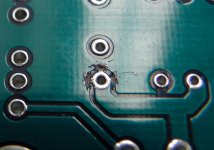
Move the cuts to the other end of the bridges next to the copper surround.
You are less likely to damage the Pad.
Ok. I am cutting it tonight.
20years or 25years neither qualifies as historical.
When did point to point wiring exist?
When did PCB first start being adopted?
When did Digital start?
When did analogue ground planes start?
When did digital ground planes start?
Your post is about modern, not historical.
Go back and read what you said in post8 from which I extracted the quote.
When did point to point wiring exist?
When did PCB first start being adopted?
When did Digital start?
When did analogue ground planes start?
When did digital ground planes start?
Your post is about modern, not historical.
Go back and read what you said in post8 from which I extracted the quote.
25 years is suprisingly long in electronics, re moores law and the cahnges we have seen over that time span. The change from throught hole to SMD, lead free, component size reduction etc etc, the move from taped up artworks to CAD generated data, the rise and fall of Gerber photoplotters, the decreasew in voltages the increase in clock speeds. My post is about designs that I did years ago as well as designs I am doing now.
All my designs have had to pass EMC, as well as working, so are tested to the nth degree, so we learn in PCB design land as we go along, and modify our practices with the time.
http://www.hottconsultants.com/techtips/split-gnd-plane.html
http://www.elmac.co.uk/pdfs/Lord_of_the_board.pdf
An intuitive, practical approach to mixed-signal grounding
http://focus.ti.com/lit/an/sbaa052/sbaa052.pdf
http://focus.ti.com/lit/ml/slyp167/slyp167.pdf
http://www.ieee.org.uk/docs/emc1206a.pdf
http://www.icd.com.au/articles/Split_Planes_AN2010_6.pdf
http://www.analog.com/static/import...gue/5467026043687049331665676350Grounding.pdf
http://www.analog.com/static/imported-files/tutorials/MT-031.pdf
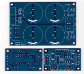
Laid out the digital and ADC boards for Syntel for this project,
(unfortenatly Syntel is now defunct) all multi layer with ground planes.
http://accelconf.web.cern.ch/accelconf/e94/PDF/EPAC1994_1551.PDF
http://accelconf.web.cern.ch/accelconf/e94/PDF/EPAC1994_2333.PDF
All my designs have had to pass EMC, as well as working, so are tested to the nth degree, so we learn in PCB design land as we go along, and modify our practices with the time.
http://www.hottconsultants.com/techtips/split-gnd-plane.html
http://www.elmac.co.uk/pdfs/Lord_of_the_board.pdf
An intuitive, practical approach to mixed-signal grounding
http://focus.ti.com/lit/an/sbaa052/sbaa052.pdf
http://focus.ti.com/lit/ml/slyp167/slyp167.pdf
http://www.ieee.org.uk/docs/emc1206a.pdf
http://www.icd.com.au/articles/Split_Planes_AN2010_6.pdf
http://www.analog.com/static/import...gue/5467026043687049331665676350Grounding.pdf
http://www.analog.com/static/imported-files/tutorials/MT-031.pdf
Laid out the digital and ADC boards for Syntel for this project,
(unfortenatly Syntel is now defunct) all multi layer with ground planes.
http://accelconf.web.cern.ch/accelconf/e94/PDF/EPAC1994_1551.PDF
http://accelconf.web.cern.ch/accelconf/e94/PDF/EPAC1994_2333.PDF
I used a cutter to cut the bridges. It was not as easy as first thought. The bridges are tiny. Cutting them is closer to a surgical operation than general DIY.
The lower C4 pad is now separated from the power ground, confirmed by the Ohm-meter. I checked that the bottom trace is electrically connected to the top pad.
What is next?
Regards,
The lower C4 pad is now separated from the power ground, confirmed by the Ohm-meter. I checked that the bottom trace is electrically connected to the top pad.
What is next?
Regards,
Attachments
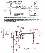
relabel the schematic.
Change all the Signal Grounds to say SG/SigRetn. R5 & C4 connect to SG
Change all the Power Grounds to say PG/PGnd.
Not shown on the PCB, but add a notional Main Audio Ground (Star) labeled MAG or Star *.
This is where the speaker return connects, not the PG.
Add the missing RF filter to the input.
Add the missing Zobel/Thiele Network to the output connected to PG.
Update the power pin decoupling to match National's recommendation.
Build up your PCB keeping those three grounds separate.
Last edited:
relabel the schematic.
Change all the Signal Grounds to say SG/SigRetn. R5 & C4 connect to SG
Change all the Power Grounds to say PG/PGnd.
Not shown on the PCB, but add a notional Main Audio Ground (Star) labeled MAG or Star *.
This is where the speaker return connects, not the PG.
Beginners like me have hard times understanding simple sentences like yours.
I hope that I relabeled correctly.
Add the missing RF filter to the input.
?
How should the missing RF filter look like?
Add the missing Zobel/Thiele Network to the output connected to PG.
Not sure about the Thiele network either. I understand that it reduces RF from and to the amp, but I am not sure about component values and configuration.
?Update the power pin decoupling to match National's recommendation.
Do not understand.
?Build up your PCB keeping those three grounds separate.
Where should the MAG be?
Regards,
Attachments
Last edited:
Nearly there.
Read National's datasheet for supply rail (power pin) decoupling.
Read National's datasheet for details of output Zobel. The 1r0 resistor comes after the Zobel R+C
The Speaker Return must be connected to MAG not PG.
When you have that, there is yet more to come.
Read National's datasheet for supply rail (power pin) decoupling.
Read National's datasheet for details of output Zobel. The 1r0 resistor comes after the Zobel R+C
The Speaker Return must be connected to MAG not PG.
When you have that, there is yet more to come.
Read National's datasheet for supply rail (power pin) decoupling.
Do not understand what the sentence means. It is regrettable that my degree is not in electronics.
Decoupling the supply rail does not evoke anything concrete in my mind.
Sorry, I will have to ask for help. Newbie here.
Read National's datasheet for details of output Zobel. The 1r0 resistor comes after the Zobel R+C.
One day, I may need to get a formal training in electronics. For now, I have to ask for some guidance. I could not find the work Zobel in the 3886 datasheet. I hope that the new corrected schematic is ok now.
MORE TO COME?When you have that, there is yet more to come.
...
I thought we were almost there...
hope not much more.
Regards,
Attachments
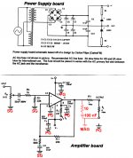
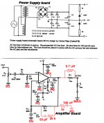
page6 Fig2.
page8 table description.
Cs is supply rail decoupling. Fig2 uses only one, but your dual polarity version Fig1 needs two.
Rsn + Csn is the output Zobel.
Adding *L // *R converts the Zobel to a Thiele output Network.
You already have the series Resistor *R. you need to add the 3 missing components.
The Output Zobel Rsn +Csn must be connected to Power Ground PG.
The speaker Return must be connected to Main Audio Ground MAG.
Read through that table. Identify every component in the Fig1 & Fig2 schematics. Find out what each component does. Ask if you can't understand any part.
Add all the extra components of Fig2 & the table to Fig1, except the single supply biasing which dual polarity does not need (Ra+Ca+Q1).
By the end of this you will be starting to understand why a chipamp with all the extras is able to do it's job.
Last edited:
Not sure about what each component does. I am lacking some basic knowledge in electronics.
As said, I am very new in electronics, even newer in audio electronics.
If swimming is all it takes to be better in audio electronics, I am posting this reply before going swimming myself.
Regards,
As said, I am very new in electronics, even newer in audio electronics.
If swimming is all it takes to be better in audio electronics, I am posting this reply before going swimming myself.
Regards,
Attachments
the Inductor (L) goes in parallel with 1r0 (R1). You don't need two resistors in series. Delete the extra 4.7mF.
m= milli (10^-3)
u= micro (10^-6)
H= Henries The inductor to use can be anywhere between 0.7uH to 3uH. Try 10 turns 1mm diameter enameled copper @ ~ 10mm diameter air cored helix
The 10r+100nF (Zobel) returns to the Power Ground PG, not MAG.
The speaker returns to MAG not PG.
Have you read the paragraph that explains each component?
Last edited:
Ok.the Inductor (L) goes in parallel with 1r0 (R1). You don't need two resistors in series. Delete the extra 4.7mF.
m= milli (10^-3)
u= micro (10^-6)
I had only copy-pasted the schematic on page 8 (Fig. 2). I was obviously wrong. Hope that this time it is correct.
Going swimming is obviously not sufficient for me to get better.
I use mu (μ) for micro. Many use u. I will use u, so that there is no misunderstanding.
Ok. I will have to find this copper helix. Maybe it can be taken from an old PCB.H= Henries The inductor to use can be anywhere between 0.7uH to 3uH. Try 10 turns 1mm diameter enameled copper @ ~ 10mm diameter air cored helix
The 10r+100nF (Zobel) returns to the Power Ground PG, not MAG.
The speaker returns to MAG not PG.
Ok.
I still have to figure out what "The Zobel should be mounted as near the output Pin and the PSU zero volts as possible" means. Also, I have not found a precise definition of Zobel network. This may explain why I cannot understand where it should be placed.
I have read it again today.Have you read the paragraph that explains each component?
Read does not mean understood, even less mastered.
Many words do not evoke anything in my mind, for instance: Q, inverting input resistance, among others.
Generally, the given functional descriptions are rather explicit, however, for a beginner, difficult to grasp why and why not placed elsewhere.
Regards,
Attachments
Hi,
I've the exactly the same PCB as the one you have.
I'm trying to implement some bass boost circuit based on this circuit
I'm wondering what I need to change?
I'm trying to understand which portion of the circuit is the bass boost.
Please help.
I've the exactly the same PCB as the one you have.
I'm trying to implement some bass boost circuit based on this circuit
An externally hosted image should be here but it was not working when we last tested it.
I'm wondering what I need to change?
I'm trying to understand which portion of the circuit is the bass boost.
Please help.
lithoc;2584183I'm wondering what I need to change?[/QUOTE said:the way you post your pics.
Reduce the pixel count. Compress using GIF and attach to your post.
Don't leave it 1800wide and on a remote server.
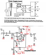
The 3886 is shown without RF filtering, without DC blocking on either the input or the NFB, without local decoupling and onboard decoupling, without a dedicated signal return to pair up with the signal input, without a delay on deactivating the mute pin, without either a Thiele output Network nor an output Zobel.
Who told the Chinese that ground planes are equal to or better than star grounding?
They actually are better if executed well. Unfortunately that is hard to do on a 2 layer board. If performed well, a ground-plane is better then a star-grounding. Inductive -wise, RF-wise and (subjective) sound-wise.
With kind regards,
Bas
the way you post your pics.
Reduce the pixel count. Compress using GIF and attach to your post.
Don't leave it 1800wide and on a remote server.
The files is at the original hosting server. Not in diyaudio site.
- Status
- This old topic is closed. If you want to reopen this topic, contact a moderator using the "Report Post" button.
- Home
- Amplifiers
- Chip Amps
- Low cost Power Amp PCB from the net (LM3886) - what do you think of the schematic?