darkfenriz said:I meant drop on Re which is pretty 'natural' phenomenon.
What is so "natural" about Re?
bocka said:Theoretical and idle current of Id = (Vt / Re*) is ideal,
Why is it ideal?
What is the equivalent in the MOSFET or jFET world?
tlf9999 said:
I have always followed the same terminology as Self used: that classes are defined by the phase of conduction, not biasing - in Class A, a device is conducting during 360 degrees of the signal. Class B, a device is conducting just 180 degrees and Class C < 180 degrees.
Once you agree with that, it is fairly logical and clear to follow his reasoning.
It is also the definition that you find in engineering texts, and what you learn at school. Any confusion here is artificially created or a result from lack of knowledge.
Jan Didden
janneman said:
It is also the definition that you find in engineering texts, and what you learn at school. Any confusion here is artificially created or a result from lack of knowledge.
Jan Didden
Thanks for confirming that my understanding is correct. Being a garbage collector, I never went to an engineering school. Wonder what exactly those folks have learnt there.
tlf9999 said:
Thanks for confirming that my understanding is correct. Being a garbage collector, I never went to an engineering school. Wonder what exactly those folks have learnt there.
Sometimes you can see it happen. Somebody talks about his class A amp with 2A of bias current. Before you know it, a lot of people think that class A means: 2A of bias current. **** happens
")
Jan Didden
I think that the effect of the gm dubling is not too big, if apply fixed resistors at the output of the VAS. This resistors makes fixed load, and there will be no changes on the open loop gain, if the output devices switch on/off.
I use this resistors, and mikeB use them too. (Mark Levinson used in the 20.5, and 23.5 as well) I have good experience with it.
sajti
I use this resistors, and mikeB use them too. (Mark Levinson used in the 20.5, and 23.5 as well) I have good experience with it.
sajti
sajti said:I think that the effect of the gm dubling is not too big, if apply fixed resistors at the output of the VAS. This resistors makes fixed load, and there will be no changes on the open loop gain, if the output devices switch on/off.
I use this resistors, and mikeB use them too. (Mark Levinson used in the 20.5, and 23.5 as well) I have good experience with it.
sajti
Sajti,
Gm doubling is caused (if it exists at all; the scientist do not agree yet), by the fact that in the xover region both output devices conduct versus just one. If both conduct, that would double Gm.
The resistors on the Vas, as far as I know, are there to give the Vas a more constant load, and to lower the influence of the varying impedance from the output reflected to the Vas.
So, yes, you are right with the open loop impact, but the Gm doubling will be there (if it is) independent of what you do to the Vas.
Jan Didden
Is it really gm doubling or currrent halfing?
In a Class B amp, let's say that you apply a voltage such that the top device outputs just 1amp and the bottom is shut off. so the load gets about 1amp current.
In a Class AB amp (overbiased Class B amp), the samem voltage generates 1amp of output current. However, since the bottom device is conducting, it is (let's assume) sucking away 0.4amp. In this case, the load gets 1-0.4=0.6amp.
In this particular example, "gm doubling" takes away the output current from the load, and reducing the "gain" so to speak.
tlf9999 said:Is it really gm doubling or currrent halfing?
In a Class B amp, let's say that you apply a voltage such that the top device outputs just 1amp and the bottom is shut off. so the load gets about 1amp current.
In a Class AB amp (overbiased Class B amp), the samem voltage generates 1amp of output current. However, since the bottom device is conducting, it is (let's assume) sucking away 0.4amp. In this case, the load gets 1-0.4=0.6amp.
In this particular example, "gm doubling" takes away the output current from the load, and reducing the "gain" so to speak.
tlf9999,
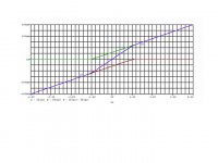
I don't think that is the reason. In all the graphs you see on Gm doubling, it is a pair of curves giving the output vs input of each device and their sum. What is shown is that at the overlap, where both conduct, the sum curve gets double steepness > double Gm.
In your example, what would happen is that the top device would conduct 1.4 amp and the bottom .4 for a 1 amp output current. If it was as you say you would have very gross xover deadband, which I think is not the case in your bias example.
Jan Didden
Edit: added a typical 'Gm doubling' pic.
Attachments
class ab biasing
Hi. I'd have to say that doug self's value of Vq of 7.18mV (cfp) is too low
for a pleasant sounding ampnce again a situation where the distorton meter says one thing and our ears another!This is probably due to the distribution of harmonics;with a higher bias it may give a higher 2nd harmonic but the 3rd and higher harmonics are much reduced.
Hi. I'd have to say that doug self's value of Vq of 7.18mV (cfp) is too low
for a pleasant sounding amp
nce again a situation where the distorton meter says one thing and our ears another!This is probably due to the distribution of harmonics;with a higher bias it may give a higher 2nd harmonic but the 3rd and higher harmonics are much reduced.Re: class ab biasing
Being a PP design (I assume), the 2nd harmonics wouldn't increase much with increased bias. It would be specifically the ODD harmonics (3rd, 5th, etc) that increase with higher bias.
So, if you like the sound better, it is for another reason as you think.
Jan Didden
p robertson said:Hi. I'd have to say that doug self's value of Vq of 7.18mV (cfp) is too low
for a pleasant sounding amp
Being a PP design (I assume), the 2nd harmonics wouldn't increase much with increased bias. It would be specifically the ODD harmonics (3rd, 5th, etc) that increase with higher bias.
So, if you like the sound better, it is for another reason as you think.
Jan Didden
Now again all of you travelled around the world and at end came to where all of you started from that too with empty handed....
No, I know how to set it in the correct way. Read my last post. Biasing ist not a question of high or low. It's a question to do it the right way.
Why is it ideal?
Read this article from Mr. Leach. Unfortunately he uses a too simplified Gummel Poon transistor model which has not so much to do with reality. And this analysis implies that you are using a voltage source as signal source. On the other side most designs use anVAS stage which has a very high output impedance, i.e. is a current source which drives the output stage.
I think there is no doubt gm ADDING does indeed exist and assuming there is a 'linearised' part of the gm curve, and you are driving the output stage from an ideal voltag source, it could be said that it is doubling - this is responsible for the rise in distortion with overbiasing. Could thje case of Re voltage being the determining factor for correct biassing, be just one of linearisation of gm curve by degeneration? It's awfully close to 25mV per Re...
That being said, there are a couple important points to note.
Firstly, we do not have a semiconductor with an ideal cut-off, so musing on class B is largely academic - class B, as defined, could indeed be usefuly employed for amplification only if the amplifying devices had ideal cut off and constant gm - the definition that a device conducts 180deg ou of the full 360 begs the definition of conduction, and we really do not have a satisfying one.
Secondly, consider the case where devices (idealized, unfortunately), conduct simultaneously when their gm is half of the nominal value - obviously, gm doubling would be highly desirable in this case as you would then ideally 'splice' the gm curves and get zero crossover distortion.
Thirdly, devices are much more interestingly nonlinear than the idealized case above, and in addition, they are not ideally complementary. At some bias point, you get minimal inflections at zero crossing, and around those points gm rise/fall does not compensate perfectly, so while it does change, you can't say that it doubles, but that it adds. Such adjustment implies least residual but it need not be harmonically 'nice'. I wonder why no-one investigates the dependency of bias adjustment with load impedance. A whole different beast would be investigating the point at which current becomes such that one device indeed goes to cut-off (such as it is), especially with a reactive load.
What he said .
Take Self's optimal bias class B with an emitter resistor of 0.1 Ohm, giving a collector current of over 200 mA. Put two each NPN and PNP in parallel, each with this collector current value. Deliver 1 Watt into 8 Ohms with it. What's the conduction angle? Not 180 degrees, that's for sure.
.Take Self's optimal bias class B with an emitter resistor of 0.1 Ohm, giving a collector current of over 200 mA. Put two each NPN and PNP in parallel, each with this collector current value. Deliver 1 Watt into 8 Ohms with it. What's the conduction angle? Not 180 degrees, that's for sure.
janneman said:I don't think that is the reason. In all the graphs you see on Gm doubling, it is a pair of curves giving the output vs input of each device and their sum. What is shown is that at the overlap, where both conduct, the sum curve gets double steepness > double Gm.
In your example, what would happen is that the top device would conduct 1.4 amp and the bottom .4 for a 1 amp output current. If it was as you say you would have very gross xover deadband, which I think is not the case in your bias example.
Jan Didden
Edit: added a typical 'Gm doubling' pic.
I think I know why. The absolute current in the crossover region is reduced: in your chart, Jan, the blue line (which represents the output current) is below (lower than) the green line which is the output of just the top device.
What happened is that gm is a dynamic idea: change in current divided by change in voltage. in the cross over region, the change in current for the same change in voltage is the sum of the change in current for the top device and the change in current for the bottom device. Thus, gm doubling.
Well, you guys with engineering degrees agree with this?
"Could this be another reason that Self's ultra low distortion "blameless" amps alledgedly do not sound nice?"
I would suggest that the problem is that all his progressively more refined designs used a regulated power supply to achieve the low THD's from simple poor PSRR designs. Then everyone builds them from the amp schematic and runs them from a simple C smoothed unregulated supply and 'lo and behold' they're listening to supply commutation artefacts! And judged not very nice.
Hi Kanwar,
I think one thing has come to light in your thread is that CFPs have lower biassing needs and so are more heatsink and low power consumption friendly while delivering linearity. Which stands to reason.
Greg
BTW, has anyone figured out what is the Vt for MOSFETs or jFETs? Don't they teach that in engineering schools?
It does not exist. The transfer characteristic of a MOSFET is different from a BJT and because of the lower gm the distortion of a MOSFET is higher when driven with a voltage source
BTW, any emitter resistor increases the distortion and more worse the distortion spectrum moves to higher orders when operating in class AB or B.
Thus, gm doubling.
No, not exactly. gm doubling is too simplified. gm changing is better. It also depends on the bias. It looks more like a wave or the overshoot of a step response.
tlf9999 said:[snip]What happened is that gm is a dynamic idea: change in current divided by change in voltage. in the cross over region, the change in current for the same change in voltage is the sum of the change in current for the top device and the change in current for the bottom device. Thus, gm doubling.[snip]
I wish I said that!
Jan Didden
janneman said:
So, yes, you are right with the open loop impact, but the Gm doubling will be there (if it is) independent of what you do to the Vas.
Jan Didden
Yes, the Gm doubling will be there. But Self sad, that Gm doubling results changes in the open loop gain, which can means distortion, or oscillation (increased feedback ratio). In my amplifier there is 5% of changes in the open loop gain if the load varies from open output to 4ohm. And this resulted by the VAS resistors.
Do You know any other effect of the Gm doubling?
sajti
- Status
- This old topic is closed. If you want to reopen this topic, contact a moderator using the "Report Post" button.
- Home
- Amplifiers
- Solid State
- low-biasing or high biasing in Class-AB amps