Your latest schem has a remote possibility of working if Q34/Q31 are Vbe matched and temperature coupled, and R19 is twice the size of R6. Then I(R74) would determine VAS quiescent. To get a high enough VAS quiescent you would either make R74 lower, which would help with the CCS, or parallel transistors onto Q31. Perhaps you could carefully increase V(R19) in 27mV increments which doubles VAS quiescent each time due to logarithmic Vbe. This may actually work if you make sure to thermally couple and match within a few mV.
All this applies to the respective component compliments of course.
Q2 and Q6 see a 1.5k impedance from their bases, which will probably cause sticking on clipping and possibly bad slewing behavior. I would bypass R1/R4 with a few nFs at least to absorb Ib spikes.
On the OLG plot, your phase goes waaaaaay past -100 which is considered a good compromise for performance and stability on most amps. Your amp has almost no open loop BW limiting. UGBW is just below 10MHz, usually it's more like 1MHz. Lower your max timestep to 100n or 10n. Sometimes the timestep in LTSpice causes loss at the frequencies your circuit would oscillate because it is so much longer than the wavelength of the frequency of oscillation.
Furthermore, you need to remove the input LP filter; the amp is seeing a filtered source so you're seeing the filter as well as the amp. The method in loopgain2.asc would not have this problem.
About the CCS. Q24/28 have an Ic of less than 150uA. The Ib from Q30 and Q35 are something like 26uA combined; almost 20% of your CCS bias current is feeding the bases. This makes for very poor CCS output impedance. A bias of at least a few mA would swamp out Ib and give the CCS much better margins and performance.
As for LTP resistors, I've put them in, and taken them out. 100 Ohm was the value I originally tried, and with this particular circuit, they didn't seem to make much difference one way or the other, either in open loop gain or closed loop gain or performance in general.
As for compensation capacitance, who knows what it will actually be once the circuit is laid out and soldered up. For simulations, that's what worked.
301K feedback resistor with a JFet device is quite reasonable.
Some one once commented that in a simulation you can balance a pencil on its point. Your simulation does not include trace inductance, stray capacitance etc. etc. If you can find a stable audio amp anywhere in the world with a 1pF feedback capacitor then I would love to see how they do it. Your open loop looks about what I would expect for a seriously under-compensated amp. The closed loop also looks believable, that is, unstable.
What you need to question is any results that look like it will work as it is.
Then you can check for other aspects like the noise of your 10k feedback shunt resistor.
Best wishes
David
Your latest schem has a remote possibility of working if Q34/Q31 are Vbe matched and temperature coupled, and R19 is twice the size of R6. Then I(R74) would determine VAS quiescent. To get a high enough VAS quiescent you would either make R74 lower, which would help with the CCS, or parallel transistors onto Q31. Perhaps you could carefully increase V(R19) in 27mV increments which doubles VAS quiescent each time due to logarithmic Vbe. This may actually work if you make sure to thermally couple and match within a few mV.
All this applies to the respective component compliments of course.
Q2 and Q6 see a 1.5k impedance from their bases, which will probably cause sticking on clipping and possibly bad slewing behavior. I would bypass R1/R4 with a few nFs at least to absorb Ib spikes.
On the OLG plot, your phase goes waaaaaay past -100 which is considered a good compromise for performance and stability on most amps. Your amp has almost no open loop BW limiting. UGBW is just below 10MHz, usually it's more like 1MHz. Lower your max timestep to 100n or 10n. Sometimes the timestep in LTSpice causes loss at the frequencies your circuit would oscillate because it is so much longer than the wavelength of the frequency of oscillation.
Furthermore, you need to remove the input LP filter; the amp is seeing a filtered source so you're seeing the filter as well as the amp. The method in loopgain2.asc would not have this problem.
OK, step by step here. First, I am unsure which two transistors you say need to be Vbe matched and thermally coupled. You mention Q34 but I just don't see that one. There is a Q24 in the general vicinity. I will also utilize the emitter resistors of the VAS transistors Q31 and Q29 to make sure that the quiescent current in VAS is in the 20-30mA range.
I'll lower the value of R74 to increase the supply current to the CCSs. That just makes sense. Changing from 1000K to 100K bumped up the current sources a couple tenths of a mA.
You mention putting capacitance across the 1.5K Ohm resistors that are used to set the cascode bias voltage on Q2 and Q6. As soon as I added even 1000pF, the output broke into oscillation. I ran a sim to clipping levels without the caps, and there was no indication of any sticking. They're being fed by current sources so perhaps the "sticking" isn't as much of an issue. Slewing behavior seems excellent as well without the caps. And as for taking care of IB spikes, during 50KHz square wave sims, the current in the 1.5K resistors went from around 2mA and spiked to 5mA on the transitions.
The input filter was (basically) removed for the Bode Plots. If you look closely, the cap value there has been set to .00068pF from its normal 68pF. If there's a difference in phase or amplitude with it in or out, I can't see it. At .00068pF, it just doesn't contribute enough phase to matter.
Some one once commented that in a simulation you can balance a pencil on its point. Your simulation does not include trace inductance, stray capacitance etc. etc. If you can find a stable audio amp anywhere in the world with a 1pF feedback capacitor then I would love to see how they do it. Your open loop looks about what I would expect for a seriously under-compensated amp. The closed loop also looks believable, that is, unstable.
What you need to question is any results that look like it will work as it is.
Then you can check for other aspects like the noise of your 10k feedback shunt resistor.
Best wishes
David
I don't doubt any of that David. But this wasn't supposed to be a critique of the amplifier design. It was supposed to be a discussion on how one could determine stability margins from the Bode Plots. Everything changes once it gets built, but that has little to do with how to interpret a Bode Plot.
Don't get me wrong, as I appreciate the suggestions that you guys have made, especially the cascode VAS stage, but I'm still trying to understand how the open loop Bode Plot can be used to determine where to set the gain and compensation to predict a stable loop.
Making the amp work after it's soldered up is a whole 'nuther topic, and I have no illusions about my potential problems. I've designed and built enough circuits over the years to realize that it's rare to hit something on the first attempt.
I meant Q24, not Q34.
Bottom line is, your circuit is unstable, it's just it won't break into oscillation in the simulator for some reason. Have no fears. It IS unstable.
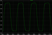
Most useful signal generators have a risetime of below 10nS. Mine has 6nS. The LTSpice square source risetime cannot be smaller than the maximum timestep - in most cases anyways. This means your current risetime is 1uS - pretty slow. So for testing with square waves set your square source to a risetime of 10nS, your max timestep to 10nS, and input frequency to 200KHz or so to avoid graph zoom cramps.
You've come up with one of those magical schematics that works wonders in simulation but shoots flames in real life. If you make sure it's stable though, it may actually work and I think it would be fun to mess with.
Before changing the stability stuff, can you plot the AC output impedance? I think it's funny that this circuit doesn't oscillate in simulation and I'm curious.
The 1p/301k resistor has a corner frequency of about 500KHz so it's effect is quite large even though it's so small.
Bottom line is, your circuit is unstable, it's just it won't break into oscillation in the simulator for some reason. Have no fears. It IS unstable.
Most useful signal generators have a risetime of below 10nS. Mine has 6nS. The LTSpice square source risetime cannot be smaller than the maximum timestep - in most cases anyways. This means your current risetime is 1uS - pretty slow. So for testing with square waves set your square source to a risetime of 10nS, your max timestep to 10nS, and input frequency to 200KHz or so to avoid graph zoom cramps.
You've come up with one of those magical schematics that works wonders in simulation but shoots flames in real life. If you make sure it's stable though, it may actually work and I think it would be fun to mess with.
Before changing the stability stuff, can you plot the AC output impedance? I think it's funny that this circuit doesn't oscillate in simulation and I'm curious.
The 1p/301k resistor has a corner frequency of about 500KHz so it's effect is quite large even though it's so small.
Okay Pete, let me calm down enough to hopefully answer your real question. Sorry, I think we are all in "circuit savior" mode.
Open-loop gain usually starts out flat at DC, and then goes on to some corner frequency. If you use ordinary miller compensation, it will drop at 6db/oct from that corner frequency onward with a phase lag of 90 degrees, like lowpass filter. If phase is within 180 degrees of zero, the circuit is stable because the feedback signal arrives with the same polarity as the input signal, though perhaps a bit early or late. Past 180 degrees, you're guaranteed oscillation because the feedback signal is now of the wrong polarity and you have positive feedback instead of negative.
At some point along the 6db/oct curve there is another corner and phase goes beyond 180 degrees. If your amp has a gain of 1 or more at this point, it will oscillate. So positive feedback at gains of less than 1 is not a problem.
We compare stability using the idea of "phase margin". Phase margin is how close the OLG phase is to 180 at the 0db (gain of 1) point. This is a useful convention. In theory, you could set phase margin to 1 degrees (179@0db) and your circuit would be stable. However it would have a resonance peak as the amplifier is resonating with its own parasitics. A phase margin of 90 degrees theoretically would have no peaking and be phase linear, but we usually go for 100 degrees because frequency response is still good enough, and this gets our miller cap significantly smaller and reduces distortion.
There are many advanced circuits where some of these things don't apply. For instance there is Two-pole miller compensation and other types that have a higher OLG corner frequency. But this is the general idea.
Also, right-click on the phase scale and set it to wrap phase. After all -270 degrees is the same as +90 degrees. This may solve some confusion.
Last edited:
I meant Q24, not Q34.
Bottom line is, your circuit is unstable, it's just it won't break into oscillation in the simulator for some reason. Have no fears. It IS unstable.
Most useful signal generators have a risetime of below 10nS. Mine has 6nS. The LTSpice square source risetime cannot be smaller than the maximum timestep - in most cases anyways. This means your current risetime is 1uS - pretty slow. So for testing with square waves set your square source to a risetime of 10nS, your max timestep to 10nS, and input frequency to 200KHz or so to avoid graph zoom cramps.
You've come up with one of those magical schematics that works wonders in simulation but shoots flames in real life. If you make sure it's stable though, it may actually work and I think it would be fun to mess with.
Before changing the stability stuff, can you plot the AC output impedance? I think it's funny that this circuit doesn't oscillate in simulation and I'm curious.
The 1p/301k resistor has a corner frequency of about 500KHz so it's effect is quite large even though it's so small.
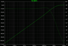
I'm not so sure it is unstable. Here's the latest closed loop plot I generated using a bit more compensation, 2.2pF instead of 1pF. From my limited recall, it appears that this plot has at least 45 degrees of phase margin.
I've also included the output impedance as well.
I don't really see any reason to drive 200KHz square waves with 10ns rise times. This amp is slew limited to somewhere between 40 and 50V/us. And with the input LPF, there's really no time it would ever see such rapid rise times. Even so, I went ahead and set time step to 10ns as well as the rise and fall times of the 50KHz square wave.
Attachments
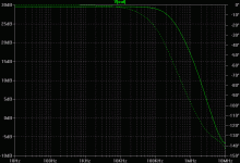
Output AC response phase at 1db gain may be different from OLG response especially at 10MHz and with phase lead compensation (1pF cap).
It looks like your circuit really is stable with this configuration, if you could manage parasitics. Changing the feedback network from 10k/300k to 1k/30k and the 1p cap to 10pF would help.
According to conventional wisdom your circuit should oscillate. I'm drawing my own simulation because I want to get to the bottom of this.
... It was supposed to be a discussion on how one could determine stability margins from the Bode Plots.
I think you have determined correctly - that the amp is unstable. I think that the problem is not with your interpretation of the Bode plots but of your results that show the amp will work. This may be a simulator artefact. The pencil example is actually deeper than a casual metaphor. It will simulate as stable but be unstable in the real world.
I understand your point that you are interested in principles, but the fact the amp is so unrealistic makes it difficult to tell if there is any other problem. Unrealistic values make it harder to spot a suspect result by comparison with previous experience and mean I can't do much more.
Best wishes
David
Last edited:
Maybe you should describe how the pencil metaphor applies, since Pete doesn't have the knowledge to figure this out. That is the reason he asked. How can he fix the circuit if he doesn't know what's wrong?
Writing it off as a simulator artifact tells me that you don't know either, you're just guessing that the simulator is wrong because the results don't make any sense. But I think if you can't describe why the simulator is wrong, then you don't really know.
OLG@0db is -270 degrees which is actually +90 degrees. I need to review information on stability. At least it will be a learning experience.
Okay pete. I knew I was forgetting something. You can't measure actual in-circuit OLG your way because in practice, the total OLG is divided by the closed loop gain and this changes everything. That's why you MUST use the method in /examples/educational/loopgain2.asc from your LTSpice directory (comes default with the program).
So, the circuit IS theoretically stable. The loopgain analysis checks out.
The reason the 1.5k resistors are MANDATORY is that they eliminate the cascoding effect at RF so that the miller capacitance of the VAS causes stability. It is not obvious, but it works.
So, the circuit IS theoretically stable. The loopgain analysis checks out.
The reason the 1.5k resistors are MANDATORY is that they eliminate the cascoding effect at RF so that the miller capacitance of the VAS causes stability. It is not obvious, but it works.
Attachments
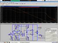
To generate loop gain, I put a 1F capacitor at the (-) input to ground to basically short it out without removing the DC portion.
I'll check out their suggested method and see if it does anything different.
Although Keantoken has given you the answer, the suggested method can go unappreciated, may I suggest you sneak up on it.
The 1F capacitor you used essentially also removed the miller compensation of the 1pF cap, as it too is now shunted to ground.
If you split R5 into 2 series resistors say 50K from the output, then place your 1F cap to ground and continue with 250K to the - input (to join the 10K and 1p miller cap) you will still have the miller capacitor in place. The resulting "open loop" should be a lot closer to Keantokens plot.
The next progression may be to insert an ac voltage source in series between the "out" and the right side of the R5 (301K) feedback resistor. Use this ac source to excite (set the input source to 0) and plot the ratio of the voltages on each side of the ac voltage source. This should get you even closer to Keantokens.
Thanks
-Antonio
Ding ding ding!!! I can't believe I missed that. But you are exactly right. Adding the extra resistor in the feedback path before shunting the net with the 1F cap did match up with Keantoken's sim. The open loop picture I was looking at was wrong, wrong, wrong, at least with the FB compensation in place.
At least we know it's not the simulator not oscillating even though it supposedly should have.
Much thanks guys. Mystery solved.

... I can't tell from the schematic how you're deriving loop gain, I suggest you might be doing it wrong like djoffe says. Look in the /example/loopgain2.asc file in the LTSpice directory and use that method.
So the problem would have been solved immediately if Keantoken's advice was followed?
...The 1F capacitor you used essentially also removed the miller compensation of the 1pF cap...
Antonio
Hi Antonio, neatly explained. The LTspice method seemed a bit complex but this thread shows why. Nice to learn.
Best wishes
David
...A phase margin of 90 degrees theoretically would have no peaking and be phase linear...
My previous post was only intended to be a preamble, but I was interrupted so here is the real question.
In a 2nd order filter the phase linear response (or best approximation, to be pedantic) is not the same as the best unpeaked response. How does this relate to phase and slope of closed loop plots? Or do I need to reread Bode and think?
Best wishes
David
I seriously don't understand the analysis method that Kean and most are using.
Still throwing a huge simulated inductor at my feedback path, to break the loop
for AC, without permitting DC to swerve into lala-land. From there, its easy to
compare input to output, and Bode plot the open loop gain and phase shift.
Between these methods, not really sure whats supposed to be the difference?
Last edited:
Kenpeter, the difference is the reason Peter's OLG plots were wrong at the beginning of the thread. The feedback loop modifies OLG; that is the whole reason opamps are either unity stable or not. When you close the feedback loop you subtract CLG from OLG. Poles in the CLG response affect OLG phase and so phase lead compensation is one way to stabilize an amplifier. Middlebrook et al developed the loopgain2.asc method to account for the affect of CLG on OLG.
Dave, phase linearity is affected by any poles in the amplifier compensation design. Compensation loading determines differential voltage at high frequencies, and so if compensation loading is phase linear, the amplifier's response will be. This is why simple miller compensation is usually pretty successful at small-signal phase linearity. It is easy to goof up phase linearity by applying feedback and compensation tricks. I'm guessing I understood your question?
I'm pretty poor on math and theory. I confess I haven't read about it directly since I don't have readily accessible study materials.
I see the optimization of square wave plots as somewhat superficial because a subjectively pleasant square wave does not guarantee phase linearity. But I do think if you can make a circuit phase linear in simulation with known good models then the results should transfer to real life. It's often argued that ultrasonic and RF step response is not important but if we worry about it anyways I think it's phase linearity we should be looking at above all else.
- Status
- This old topic is closed. If you want to reopen this topic, contact a moderator using the "Report Post" button.
- Home
- Amplifiers
- Solid State
- Loop stability clarification . . .