I would not want my IV current limiting @ 2.7Apk.
That is ~1.9Aac and would result in ~29W of output into 8r0 at the limit.
It will start to interrupt the signal when Ie~1.8Apk and that is just 13W of output into 8r0.
As Vce rises, when feeding a reactive (speaker) load, the current limit will come in even sooner.
That is ~1.9Aac and would result in ~29W of output into 8r0 at the limit.
It will start to interrupt the signal when Ie~1.8Apk and that is just 13W of output into 8r0.
As Vce rises, when feeding a reactive (speaker) load, the current limit will come in even sooner.
Transistors overheating
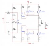
This is the current schematic I have been working on.
I have raised the supply voltage to +/- 12V. The input signal is +/- 9V. The expected load is 22R.
On the prototype one output transistor gets hot. Once one or two transistors get hot, the current consumption increases.
Being a prototype I have the smallest coolers on the transistors and not thermally together. I understand that putting them all on the same heatsink shares the heat and prevents one from running away. I had also thought that the 0.1R emitter resistors were there to prevent such a runaway, but they do not. I have even tried to increase the emitter resistor to no avail, once a transistor gets hot, it remains hot.
So it seems the common heatsink is the way to go, but would like to know if there is a way to do it without common heatsinks?
Edit: measured temperatures are about 45C-65C for the hot transistors and 35C for the cold ones. In cases one of the hot transistors has clocked 85C. I usually power down when something gets so hot.
Attachments
Last edited:
The Vbias transistor Q7 needs to be thermally connected to one of the driver transistors Q2 or Q3 . Mount Q7 back to back with either Q2 or Q3 and secure together with a cable tie . The positive rail output transistors can share one heatsink and the negative rail outputs can share another one . The drivers can each have their own individual heatsinks .This separation of devices and heatsinks is possile because you are using a complementary feedback output stage configuration.
In my practical topology, heating Q7 with the tip of the soldering iron, works as expected and reduces the bias.
However the drivers Q2+Q3 run very cool (while one of the output transistors is burning) and they would have no effect on Q7. I think it would be better to connect thermally Q7 with the output transistors, if they were all on the same heatsink.
What I am still not getting is the runaway effect: one of the outputs runs away, and it seems I cannot stop it with the emitter resistor but all the designs I have seen is to mount sometimes dozens of transistors in parallel and use the emitter resistor for balance.
Why is mine not balanced? It may be the lack of heatsink causing this. I will have to build a proper prototype on a large heatsink.
Yes it should be more than fast enough, but it is built on a breadboard and maybe is suffering lots of parasitic capacitances. I let it run for an hour yesterday and I had two transistors at 40C and two at 60C. I think without a proper heatsink all measurements are worthless. The only way is to build it and see.
Temporarily remove one output pair, (disconnect one end of each emitter resistor).
Check the CFP then biases correctly.
Better to thermally couple Q2, 3 & 7. A short thick strip of aluminium or copper. Just glue the three flat faces to the strip.
Check the Multiplier output voltage and compare that voltage to the driver collector resistor currents. You should see the two following exactly, and not running away as the circuit warms up.
- Status
- This old topic is closed. If you want to reopen this topic, contact a moderator using the "Report Post" button.
- Home
- Amplifiers
- Solid State
- Load and device protection