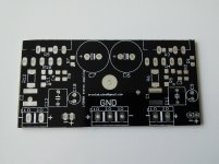
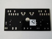
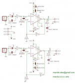
Just wanted to share with you my LM3886 stereo PCB with mainly 1206 smd size components. Some components have Farnell ordering codes in schematic for easier sourcing.
Best Regards,
Aleš
Best Regards,
Aleš
Attachments
Nice work. Thats interesting layout.
But i see a few problems:
Aren't feedback resistances too low? Thats basically 1K from output to gnd. 10s of miliamps will be flowing through them.
100nf decoupling caps are too far from LMs (C5 & C8).
There is no Mute cap. Danger of pops when turned on.
I would route C7&C6 with separate traces to star point. But this one probably makes little difference.
Why electrolytic cap on input? R2 and R8 can be easilly increased to 47K, and then small 0.68-1uF film caps on input will be enough.
Last edited:
Thank you!Nice work. Thats interesting layout.
If you try it you'll notice that there is nothing wrong with it and the sound of chipamp will vastly improve.But i see a few problems:
Aren't feedback resistances too low? Thats basically 1K from output to gnd. 10s of miliamps will be flowing through them.
You're right about C5 and C8 but this was the best option to use only two for both of the LMs. You're also right about routing GND from C5, C6, C7 and C8 to star point, I didn't see it before.100nf decoupling caps are too far from LMs (C5 & C8).
There is no Mute cap. Danger of pops when turned on.
I would route C7&C6 with separate traces to star point. But this one probably makes little difference.
I tested the PCB and I didn't have any turn on/off pops.
It is tantalum 10uF/16V capaitor in paralel with 10nF MKP1837 capacitor. I found this combination more neutral than any other foil capacitor and very good sounding.Why electrolytic cap on input? R2 and R8 can be easilly increased to 47K, and then small 0.68-1uF film caps on input will be enough.
Why?you need caps for both the rails for both the chips.
You're absolutely right, I should have placed it next to R3 and R9. Trace would be then as short as possible. Still It can be solved with through hole resistor soldered directly to the pins of LMs.fb resistor r5 is too far.
How would this improve the sound quality?rf filter should be close to input socket.
Best Regards,
Aleš
Last edited:
Not good... Not good at all... Missing HF filters on supply rails. There's more than that tho...
Please elaborate why is it not good at all.
I couldn't call it a good design because:
Poor grounding, think and long supply rails, no HF filters on both chips, signal layout should be as compact and as closely together as possible and as far away from output and supply rails as possible and missing mute cap. I'm not an expert on this but just second opinion. Which is all true")
BTW, have you tried your PCB's yet? I wouldnt risk. Chips wont blow up but they will oscillate for sure.
Poor grounding, think and long supply rails, no HF filters on both chips, signal layout should be as compact and as closely together as possible and as far away from output and supply rails as possible and missing mute cap. I'm not an expert on this but just second opinion. Which is all true
BTW, have you tried your PCB's yet? I wouldnt risk. Chips wont blow up but they will oscillate for sure.
you need caps for both the rails for both the chips.
Why?
Because the way you have done it now, you get very poor channel separation.
How would this improve the sound quality?
Best Regards,
Aleš
I guess because you would want the rf to goto ground asap. Thats why people solder a cap to the chassis input socket also, along with the resistance of the interconnect, it acts like an rf filter.
Last edited:
I couldn't call it a good design because:
Poor grounding, think and long supply rails, no HF filters on both chips, signal layout should be as compact and as closely together as possible and as far away from output and supply rails as possible and missing mute cap. I'm not an expert on this but just second opinion. Which is all true
BTW, have you tried your PCB's yet? I wouldnt risk. Chips wont blow up but they will oscillate for sure.
You are clearly mistaken, PCB has excelent grounding because every components ground is routed into star point. Which HF filters you are reffering to, the ones on the input?
I could place components on the input better but hey this isn't bad also. Missing input cap doesn't make desing good or bad. I have one LM3886 without this mute cap for over 10years now and no turn on off pop noise is present.
Yeah I tried this PCB and no oscillations are present, no noises etc. and the sound is awesome. You are forgetting that this chip can work with very little amount of components stable.
it works doesnt mean it cannot be made better.
All grounds are not same. You need to have a separate ground point for input signal.
Keep your output away from power.
Make your signal stage as compact as possible. Protect it with a ground pour. Make your current loops as small as possible.
If you can see connections when you are placing the components, use it as a guide when placing devices. Your placement could be optimise quite a lot, an example is R2, R4, R5 & C3, have a good look at their connectivity, with a few minor tweaks you would have a much better layout. Don't go with your first or even 3rd or 4th attempt, have a play and look at how the routing pans out for different placement.
When laying out power and decoupling caps come first, feedback comes second then the rest.
As to the spiders legs GND, yuk, but I wont get into discussions on that, other than to say it does look like a very nice antenna, adds lots or parasitic inductance and resistance to signal returns.
Other than that I do applaud you for going with SMD, it would be nice to see more use such devices, and keep practicing placement and seeing how the routing evolves with different placement.
it works doesnt mean it cannot be made better.
All grounds are not same. You need to have a separate ground point for input signal.
Keep your output away from power.
Make your signal stage as compact as possible. Protect it with a ground pour. Make your current loops as small as possible.
Of course they are not, but at some point they must be connected together, in my case this is in the star ground. GND current loop is minimised.
I came to the point where little things don't make such huge difference anymore.Little things make huge difference.
If you can see connections when you are placing the components, use it as a guide when placing devices. Your placement could be optimise quite a lot, an example is R2, R4, R5 & C3, have a good look at their connectivity, with a few minor tweaks you would have a much better layout. Don't go with your first or even 3rd or 4th attempt, have a play and look at how the routing pans out for different placement.
When laying out power and decoupling caps come first, feedback comes second then the rest.
As to the spiders legs GND, yuk, but I wont get into discussions on that, other than to say it does look like a very nice antenna, adds lots or parasitic inductance and resistance to signal returns.
Other than that I do applaud you for going with SMD, it would be nice to see more use such devices, and keep practicing placement and seeing how the routing evolves with different placement.
Yes, signal components could be routed much better.
Other than saying yuk, have you calculated parasitic inductance and resistance on this PCB? Do we know how other LM3886 designs perform regarding parasitic components? How much of this parasitic components is added by wires from connectors to PCB?
Antenna for what frequencies?
Best Regards,
Aleš
I don't do spiders legs grounds on any Analogue PCB I do, I have never seen that style of routing anywhere other than DIY audio, it is horrible, but seems to be the fashion for DIY Audio. As said I only see this style of routing for DIY audio no where else.
Less dramatic splitting of the ground would be better, power, signal etc.
Wires are a different story and provide their own problems/solution we are talking on board (the layout is where EMC/signal integrity solutions start) where you have feedback loops (critical) etc.
Todays world is polluted by RF noise, to get a better understanding I would suggest you read something like Henry Otts "Electromagnetic Compatibility Engineering".
A lot of the work, simulating and actual testing has been done:
Taming the LM3886 Chip Amplifier
a la our tomchr !
Taming the LM3886 Chip Amplifier
a la our tomchr !
I don't do spiders legs grounds on any Analogue PCB I do, I have never seen that style of routing anywhere other than DIY audio, it is horrible, but seems to be the fashion for DIY Audio. As said I only see this style of routing for DIY audio no where else.
Then you should definitely check NAIM audio. You can't just say it is horrible. From diy aspect is way better than most of the designs, why? Most of LM3886 PCB out there are mono designed which means that to achieve best sound of it we would need separate PSU for each channel. What I see among diyers, is that two of mono PCBs are in most cases used with one PSU for both channels. And then all the troubles appear, from hum, to brum, to bad sound quality. The biggest mistake made is when two star grounds are connected together.
Less dramatic splitting of the ground would be better, power, signal etc.
Actually I tried this prior to this design and I must say this one is better. The concept here was to bring GND from every component to star ground and to reduce feedback resistor value.
Wires are a different story and provide their own problems/solution we are talking on board (the layout is where EMC/signal integrity solutions start) where you have feedback loops (critical) etc.
Todays world is polluted by RF noise, to get a better understanding I would suggest you read something like Henry Otts "Electromagnetic Compatibility Engineering".
I have a very good understanding about RF noise. If casing is properly shielded there shouldn't be much noise. Also what about every wire in the signal line?
Unfortunately I've read this when I already had PCB in fabrication. I would have made some things on PCB a lot better.A lot of the work, simulating and actual testing has been done:
Taming the LM3886 Chip Amplifier
a la our tomchr !
Tom did a very good job but again he is focusing on mono LM3886. I would be very much interested in some real measurements.
BR,
Aleš
If the case is properly shielded, EMC still starts with good PCB design.
I can, it is overdone on DIY audio. I do very little commercial audio work, and don't really need to look at NAIM audio...
I do layout for professional audio and many more sensitive analogue designs and as I have said the only place I see this spiders legs type layout is on DIY audio designs, no where else where analogue design is used.
You have stated this correctlyWhat I see among diyers, is that two of mono PCBs are in most cases used with one PSU for both channels. And then all the troubles appear, from hum, to brum, to bad sound quality. The biggest mistake made is when two star grounds are connected together.
You have stated this incorrectly.I have a very good understanding about RF noise. If casing is properly shielded there shouldn't be much noise. Also what about every wire in the signal line?
Cables from the outside to the inside, bring the interference to the inside of the enclosing screen. You have to do something in addition to providing the screening enclosure.
Multi-channel amplifiers are more difficult to get right than Monoblocks............ I would have made some things on PCB a lot better.
Tom did a very good job but again he is focusing on mono LM3886. I would be very much interested in some real measurements. ...........
I have NEVER got a chassis enclosed amplifier quieter than a bare prototype on the test bench.
I have NEVER got a two channel amplifier quieter than a Monoblock.
- Status
- This old topic is closed. If you want to reopen this topic, contact a moderator using the "Report Post" button.
- Home
- Amplifiers
- Chip Amps
- LM3886 with SMD components