Hi, I have zipped the schematic and board files allong with the library file for the LM3886 chip and attached it below. You may find that you will have to add the library to your list in eagle before you can view the files properly, but I doubt that that will be too much of a problem (let me know if you get stuck, and I might be able to help out).
Otherwise, enjoy!
Otherwise, enjoy!
Attachments
Hi, the version of eagle that I used to do this is FREE! You can get a coppy from thie website below if you wnat one, but if you can't do that, I guess I could come up with some black and white gif's for you (just let me know if you need them).
http://www.cadsoftusa.com/
http://www.cadsoftusa.com/
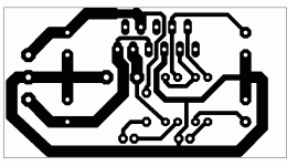
Here is the board track layout that you can use straight off, without having the software (please remebmer, that this is a top down view, so you may need to mirro it depending on how you intend on transfering it tot he bottom layer of your board).
edit:
I forgot to mention that this should be printed out at 300 DPI without any resampling of the image ofr it to come out the correct size.
edit:
I forgot to mention that this should be printed out at 300 DPI without any resampling of the image ofr it to come out the correct size.
Attachments
WOW, thats amazing for a free program.
Is it easy to use? I am going to download it, but its a 7MB file, so I'll have to wait until later. I can only spend about 20 more mintutes on the internet.
I think I can print at 300x300dpi, but if not, by any chance would you know how much to scale it down?
Thanks again for designing this!
Is it easy to use? I am going to download it, but its a 7MB file, so I'll have to wait until later. I can only spend about 20 more mintutes on the internet.
I think I can print at 300x300dpi, but if not, by any chance would you know how much to scale it down?
Thanks again for designing this!
Eagle does have it's limits (at least in the free version, of board size, and the number of layers), but it is by far the easiest program I have used for trying to design PCB's (it makes trying to learn protel even worse). Just draw a schematic, press the CAD buttoin and it will create a set of components with all of the nets conected how you want them (providing you have teh pars int eh librbary). All you have to do is place them where you want, and join up the pins (there is an auto router, but I would advise against using this for the most part).
If you do need to try and scale the picture, just print it out on a piece of paper first, and try and match up the pin hole son your 3886 with the ones in the picture (when these match, you know you have it the right size).
If you do need to try and scale the picture, just print it out on a piece of paper first, and try and match up the pin hole son your 3886 with the ones in the picture (when these match, you know you have it the right size).
the picture itself isn't supposed to be 300 pixels wide, but rather it is the corect size that when set to a resolution of 300 pixels (dot) per inch, it will be the corect size to print out.
So, if you can get fireworks to leave the picture with the same number of pixels (try selecing it so that it doesn't resample the image), and then change the resolution if the image, or i't s physical width (depending on what you have control of, I know you can do both in photoshop, as that's what I used to create it), so it is either 300 pixels per inch, or measures 2.573 inches wide by 1.487 inches high.
edit:
I have done the resizing for you and saved the image file as a tif, so it will remember the correct resolution and size of the image, so if you open this, and print it out without any resizing, it should be the correct size.
Attachments
As far as the grounding goes, all of the signal grounds are conected together before going back to the main grounding point. However, as the current draw on the signal lines will at most be a few mA there shouldn't be any problems here (you would normaly only have this sort of problem if signal and power grounds share the same path I think).
LM3886 design
Hi.. This is my first post here in DIYAudio... if my questions seem dumb, thats because i am just overenthusiastic rather than stupid... please bear with me...
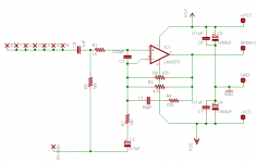
Anyway, i saw Parsnips pcb layout for the schematic on nat. semi's datasheet; and tried to come up with a design solution before i fabricated the boards...
please have a look at the component values on the below and tell me if they make a workable design.. if not, please suggest a suitable value...
Vcc/Vee : 35V
Rl : 8 Ohms
Rf : 22K Ohms
Ri : 1K Ohms
Ci : 10u Farads
Rb : 4.7K ohms
Rin : 47K ohms
Cin : 10u Farads
Thanks in advance...
Madhu.
Hi.. This is my first post here in DIYAudio... if my questions seem dumb, thats because i am just overenthusiastic rather than stupid... please bear with me...
Anyway, i saw Parsnips pcb layout for the schematic on nat. semi's datasheet; and tried to come up with a design solution before i fabricated the boards...
please have a look at the component values on the below and tell me if they make a workable design.. if not, please suggest a suitable value...
Vcc/Vee : 35V
Rl : 8 Ohms
Rf : 22K Ohms
Ri : 1K Ohms
Ci : 10u Farads
Rb : 4.7K ohms
Rin : 47K ohms
Cin : 10u Farads
Thanks in advance...
Madhu.
Right, I have had a look, and I think there are a few things you should note:
Firstly RL is the loudspeaker, so you don't need to include this in the circuit.
Secondly, you DO have to include Rm as this controls the mute function of the chip. This should be set to allow 0.5mA to flow from teh pin which I think is at ground, so for your rails (+/-35V) I think it should be about 70K, but I would check this yourself as I am probably wrong here.
Third, there is no provision for Cin, or Rin on the PCB, as Rin is the volume pot (which would be conected up to the corect pins in the PCB insted), and I didn't bother with in input cap as Soundnerd didn't want one (I think).
Fourth, I wouldn't bother changing the value of Rb, just keep it at 1K.
But appart from those few things, all of the rest of the components seem about right (although, I would be tempted to use biger caps for Cf and Cm as you can easily fit them on the baord, and the non-polar electrolytics aren't too expensive).
bigparsnip said:
Secondly, you DO have to include Rm as this controls the mute function of the chip. This should be set to allow 0.5mA to flow from teh pin which I think is at ground, so for your rails (+/-35V) I think it should be about 70K, but I would check this yourself as I am probably wrong here.
Rm on the spreadsheet is set to a default of 35K... would that be OK??? and what is Cf?? it is not in the schematic.... by the way parsnip, would you mind posting the component values you hav used for soundnerd's pcb??
Madhu.
Hi, sorry, that should be Ci, like you have listed above as being 10uF. As far as what components sound nerd used, I have no idea, you will have to hope he gives you a reply to your questions, as I have never tried to build up this PCB, only the LM3875 one for my little amp.
Oh, and 35k, would probably be fine, I doub't it has to be too close in this case, but perhaps someone with a bit more experience could give you a better idea about that.
Oh, and 35k, would probably be fine, I doub't it has to be too close in this case, but perhaps someone with a bit more experience could give you a better idea about that.
Very interesting discussion. I saw it just now. And hi, Madhu. I too am from India. ")
I've been trying to finish working on a non-inv amp using the LM3875. Other than the muting function, the schematic should be identical to what I'd use for the LM3886. (The board layout will of course be different, because the pinouts of the two chips vary.)
I too started with the first schematic on the LM3875 datasheet, and then looked at some refinements in the single-supply version of the schematic in the same datasheet, and also looked around on the Net a bit, and played around with the Nat Semi spreadsheet which they provide to let you design non-inv amps, see the power dissipation, etc. I also ran the schematic through a friend much more experienced than I. I've attached it here. I just thought that since there are at least two of you on this thread who appear to be beginners like me, we could work on the schematic together. We can then do the PCB design in Eagle (I too use the Eagle freeware, Bigparsnip, but on Linux. I like it a lot.)
The schematic I've shown here is exactly what I'll put on my PCB, once I get an okay from you guys that it'll work. The only parts external to the PCB will be the transformer and bridge rectifier. (I was thinking of using mass-market parts to build it, and not opt for the hi-tech diodes that some others seem to prefer for Gainclone bridge rects.) I want an input cap, and I omitted the RL circuit at the speaker output. Many others seem to have omitted it too, in their gainclones. From what I've understood, C8+R5 form one first-order high-pass filter and affect the lower frequency limit, and R2+C2 together act as a second first-order filter. With my values, C8+R5 will give me 0.16/(1uF * 56K), which gives me 2.86Hz. And R2+C2 gives me 0.16(10K * 4.7uF), which is 3.4Hz. So the -3dB point, as far as I've understood, will be 3.4Hz for my schematic. C1+R4 reduce the gain of the amp at high frequencies, reducing the possibility of high frequency oscillations. All this is what I've acquired in bits and pieces by pestering others (something I'm good at ) --- my own understanding of these things is minimal.
As my schematic shows, there's no connection between signal ground and power ground in this schematic, and there will not be any in the PCB. I intend to take leads from both terminals to a star ground off-board somewhere. And the return path from the speaker will also go directly to that star-ground, not to this PCB. In fact, I think I'll take the lead from the power-ground (marked GND) of this PCB back to the centre tap of the power transformer, and take a separate lead from that centre tap to the star-ground. That way, the heavy charge/discharge currents between the smoothing caps (C4 and C5 in my schematic) will not flow through the star ground.
Any comments? Please?
I've been trying to finish working on a non-inv amp using the LM3875. Other than the muting function, the schematic should be identical to what I'd use for the LM3886. (The board layout will of course be different, because the pinouts of the two chips vary.)
I too started with the first schematic on the LM3875 datasheet, and then looked at some refinements in the single-supply version of the schematic in the same datasheet, and also looked around on the Net a bit, and played around with the Nat Semi spreadsheet which they provide to let you design non-inv amps, see the power dissipation, etc. I also ran the schematic through a friend much more experienced than I. I've attached it here. I just thought that since there are at least two of you on this thread who appear to be beginners like me, we could work on the schematic together. We can then do the PCB design in Eagle (I too use the Eagle freeware, Bigparsnip, but on Linux. I like it a lot.)
The schematic I've shown here is exactly what I'll put on my PCB, once I get an okay from you guys that it'll work. The only parts external to the PCB will be the transformer and bridge rectifier. (I was thinking of using mass-market parts to build it, and not opt for the hi-tech diodes that some others seem to prefer for Gainclone bridge rects.) I want an input cap, and I omitted the RL circuit at the speaker output. Many others seem to have omitted it too, in their gainclones. From what I've understood, C8+R5 form one first-order high-pass filter and affect the lower frequency limit, and R2+C2 together act as a second first-order filter. With my values, C8+R5 will give me 0.16/(1uF * 56K), which gives me 2.86Hz. And R2+C2 gives me 0.16(10K * 4.7uF), which is 3.4Hz. So the -3dB point, as far as I've understood, will be 3.4Hz for my schematic. C1+R4 reduce the gain of the amp at high frequencies, reducing the possibility of high frequency oscillations. All this is what I've acquired in bits and pieces by pestering others (something I'm good at
) --- my own understanding of these things is minimal.As my schematic shows, there's no connection between signal ground and power ground in this schematic, and there will not be any in the PCB. I intend to take leads from both terminals to a star ground off-board somewhere. And the return path from the speaker will also go directly to that star-ground, not to this PCB. In fact, I think I'll take the lead from the power-ground (marked GND) of this PCB back to the centre tap of the power transformer, and take a separate lead from that centre tap to the star-ground. That way, the heavy charge/discharge currents between the smoothing caps (C4 and C5 in my schematic) will not flow through the star ground.
Any comments? Please?
Attachments
- Status
- This old topic is closed. If you want to reopen this topic, contact a moderator using the "Report Post" button.
- Home
- Amplifiers
- Chip Amps
- Lm3886 Pcb