Are you aware that an aerial that picks up interference is a loop?
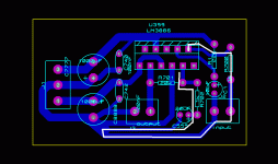
Now start at PIN9 and follow the traces and components: to R701, to R702, through R702, to C555, through C555, to star ground, to Input PIN1, to PIN2, to R700, through R700, to PIN10.
Now shade in the area enclosed within that route.
That is your loop area. That is your aerial picking up interference.
You must make that group of components and traces and pins as small and as compact as possible and try to minimise the loop area.
Repeat for the output.
Repeat for the Zobel.
Repeat for the PSU rails.
Andrew,
Thanks a lot for your reply.
Yet I do not have a good point of view about the aerials which make LOOPS!
I did know that the inputs can act as an aerial if the input wire/trace happens to be long. But yet I have no idea what you do mean here.
Plz take a look at the WHITE sign here in the below pic and let me know if I have drew it the right place to show the aerial loop you are talking about?
Thanks
P.S is the aerial loop defined just for INPUTs?
Attachments
Regarding the optional components actually I want to makes a prototype based upon the schematic in the datasheet and then I will improve it and add the optional components just if needed.
Shouldn't the PCB provide the space for all those components then? Or will you let the additional components dangle about in free air?
Those 1000 µF capacitors look pretty small. Do they have sufficient voltage rating for that amp?
Newb in need of a bit of help
I've got a set of these boards to build up and I'm okay with it appart from one thing which confuses me. Setting aside the attentuation and Zobel amendments (&argument) for a moment, what is the purpose of R1 in the circuit as it stands? I have seen other 3886 circuits which use either an 0.7mH inductor here or an inductor in parallel with a a 10 ohm resistor resistor. Indeed the datasheet itself in one schematic has a 4700mf electrolytic cap in series with the parallel inductor/resistor, although I've yet to see any implemented design using this cap. I'm thinking to leave the R1 out , insert a link and do the zobel off board. Does that make sense?
RF attenuation is omitted.
Very easy to correct: add a parallel cap across R5 either on top of the PCB, or underneath the PCB.
Output Thiele Network is omitted.
Very easy to correct: remove the output terminal block. Connect the Zobel capacitor in the spare location.
Tap off the speaker output from the top end of R1.
The other half of the Thiele Network (L//R) can be mounted offboard in the line that joins the amp PCB to the speaker terminals fitted to the chassis.
The speaker return connects to the Main Audio Ground, not to the amp PCB.
Finally,
check to see how R5 and C4 are connected to Signal Ground. They must not connect to Power Ground on the underside of the PCB.
I've got a set of these boards to build up and I'm okay with it appart from one thing which confuses me. Setting aside the attentuation and Zobel amendments (&argument) for a moment, what is the purpose of R1 in the circuit as it stands? I have seen other 3886 circuits which use either an 0.7mH inductor here or an inductor in parallel with a a 10 ohm resistor resistor. Indeed the datasheet itself in one schematic has a 4700mf electrolytic cap in series with the parallel inductor/resistor, although I've yet to see any implemented design using this cap. I'm thinking to leave the R1 out , insert a link and do the zobel off board. Does that make sense?
no sense.
The AC coupled ex sch in the Datasheet is a far better circuit. It adopts the optional components that should never be optional for a beginner project.
Just convert that sch back to dual polarity supply.
Thanks. I realized the error of my ways after posting

Hey guys.
I bought a couple of these boards a few months ago and haven't really gotten to them. Today I got my hands on a pair of speakers (for free) that would really go well with this amplifier.
Thing is I don't really know what components I should use. The PSU PCB has 4 capacitors with no values printed, and also the actual amplifier PCBs have no values at all, just numbered resistors and capacitors.
Can someone point me to the components I should use?
Hey guys.
I bought a couple of these boards a few months ago and haven't really gotten to them. Today I got my hands on a pair of speakers (for free) that would really go well with this amplifier.
Thing is I don't really know what components I should use. The PSU PCB has 4 capacitors with no values printed, and also the actual amplifier PCBs have no values at all, just numbered resistors and capacitors.
Can someone point me to the components I should use?
I used CharlieLaub's circuit and referred to the National datasheet and various other published designed to arrive at the following values for the same board.
R1 0R15 5w
R4 680 0.25w
R6 1K 0.25w
R2 10K 0.25w
R3,5 22K 0.25w
C5 1-3.3uF 100v DC block. Polyester
C1,2,3 100uF 50v electrolytic
C4 22uF 50v electrolytic
Mine work very well powering 6 ohm mid bass and 8 ohm treble units fed from an active crossover and powered by 22-0-22 traffo. The mid reproduction is superb and in my view compares very well to the much vaunted rev c which I also built. Neither give much deep bass slam.Most designs have a zobel at the output which I omitted for 2 reasons. Firstly it wasn't the designer of the pcb's intention but also I came across some designs where the designer added a zobel and then removed it because it had a deleterious effect on the sound. Likewise most design have a 220pf cap across pins 9 and 10 for rf attentuation. I also omitted this primarily because I wanted to see if I could hear any rf on the circuit as it stands, which I can't. If you want to add a zobel the followinglink may prove helpful.
http://www.eetimes.com/document.asp?doc_id=1274906
Last edited:
Andrew,
Thanks a lot for your reply.
Yet I do not have a good point of view about the aerials which make LOOPS!
I did know that the inputs can act as an aerial if the input wire/trace happens to be long. But yet I have no idea what you do mean here.
Plz take a look at the WHITE sign here in the below pic and let me know if I have drew it the right place to show the aerial loop you are talking about?
Thanks
P.S is the aerial loop defined just for INPUTs?
I worry that you will not be able to get your LM3886 flat against a heatsink unless you place the bottom of the heatsink above the board so the board slips under the sink a bit. Dangerous- as in for sure you will have a short. Of course I suppose you might have the copper on the bottom side but still to me its odd to have the board sitting under the sink.
You live dangerously, or rather you let your amp live dangerously...............Most designs have a zobel at the output which I omitted for 2 reasons. Firstly it wasn't the designer of the pcb's intention but also I came across some designs where the designer added a zobel and then removed it because it had a deleterious effect on the sound. Likewise most design have a 220pf cap across pins 9 and 10 for rf attentuation. I also omitted this primarily because I wanted to see if I could hear any rf on the circuit as it stands, which I can't. If you want to add a zobel the followinglink may prove helpful.
IC Audio Power Amplifiers and Zobel Networks: One Size Does Not Fit All | EE Times
The EE times article is discussing the effect of a speaker Zobel fitted at the speaker and the effect that combination has on the amplifier.
That is a very different situation from the amplifier output Zobel that is provided at the amplifier to provide a defined HF load that aids amplifier stability.
Fit an amplifier Output Zobel. National define the components for you.
You live dangerously, or rather you let your amp live dangerously.
The EE times article is discussing the effect of a speaker Zobel fitted at the speaker and the effect that combination has on the amplifier.
That is a very different situation from the amplifier output Zobel that is provided at the amplifier to provide a defined HF load that aids amplifier stability.
Fit an amplifier Output Zobel. National define the components for you.
To be clear, the output zobel you are referring to is the 4700uf electrolytic, 0.7 mH inductor and 10ohm resistor shown at the output of pin 3 in Fig 3 of the National datasheet, yes?
The Zobel network is a low-value resistor and low-value cap in series, from output to ground. It should be connected as close as possible to the amplifier output, and directly to the load ground.
The Zobel network is sometimes also called a Boucherot cell, although I have usually seen the Boucherot cell referred to as the parallel inductor and resistor that are in series with the output, combined with the Zobel network from output to ground.
By the way, it is not a good idea to wrap the inductor's wire around the resistor, to make the low-value inductor that goes in parallel with the resistor.
Last edited:
The Zobel network is a low-value resistor and low-value cap in series, from output to ground. It should be connected as close as possible to the amplifier output, and directly to the load ground.
The Zobel network is sometimes also called a Boucherot cell, although I have usually seen the Boucherot cell referred to as the parallel inductor and resistor that are in series with the output, combined with the Zobel network from output to ground.
By the way, it is not a good idea to wrap the inductor's wire around the resistor, to make the low-value inductor that goes in parallel with the resistor.
Thanks Goatee. I was trying to work out how Andrew T's mods at post 22 to the XY pcb and schematic at post 21 relate to any of the schematics in the National Datasheet. In fact I was looking at fig 3 of the TI datasheet which = fig 2 of the national datasheet.
Think I have it more from Rod Elliott's 3886 schematic. If I have understood this correctly R6 on Rod's schematic = R1 of the aformentioned pcb, (and in my build at least needs to be changed in value to 2R7). C4 on Rod's schematic is the cap which Andrew would have soldered onto the XY board in place of the speaker in/out block terminal and it returns to the XY pcb 0V line. Andrew T would then tap off a line to the speaker from the top of R6/R1 and add a paralelled inductor and resistor in series to the speaker input returning the speaker output to MAG.
A picture speaks a thousand word so I have attached Rod's original circuit and a version of how I understand it relates to post 21 and 22.
Attachments
I think that the schematic would stay almost the same, except for the addition of a 220 pF-or-so cap in parallel with R5 (R1 on Rod Elliot's schematic), the 22k input resistor.
AndrewT was talking about modifying the PCB, in order to accommodate the schematic. i.e. In order to add the L1 and R5 on Rod's schematic to the PCB.
I think that what you have drawn is correct. But when you say "speaker tap off", it's a little confusing. The speaker will still connect to where it says "OUT1" on your schematic, which will now be a jack mounted in the chassis. The parallel R5 and L1 in your schematic will be dangling in the wire between the output and the speaker jack.
Hi,
You are looking for ready PCB, or want to make your own ?
Sudheer, after a layoff doing other things, I'm about to make a couple of my own Thiele output network pcbs along Greg Erskine's lines. If they seem okay, i.e. the amps are stable and without any noticeable sound degradation I will try and do the Andrew T mods to the XY boards, if my hands are steady enough (I have a disability which pretty much limits what intricate work I can do). Any hints/tips gratefully received. Thanks.
- Status
- This old topic is closed. If you want to reopen this topic, contact a moderator using the "Report Post" button.
- Home
- Amplifiers
- Chip Amps
- LM3886 PCB