This thread will chronicle development of an amp that blatantly rips off the optocoupler-mediated current source used in the GeneSic amp investigated by Papa in another thread. http://www.diyaudio.com/forums/pass-labs/283611-zen-ga10jt12.html
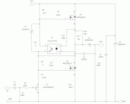
Not liking amps with only a few ohms of input impedance, I substituted a buffered "Fake SIT" for the GeneSic device. The resulting amp should be much easier to drive. Sound? I'll find out, sooner or later. This is a placeholder until I get around to attaching supplemental material. Layout is pretty much done, so I will need to pencil in some appropriate component values in order to proceed.
Not liking amps with only a few ohms of input impedance, I substituted a buffered "Fake SIT" for the GeneSic device. The resulting amp should be much easier to drive. Sound? I'll find out, sooner or later. This is a placeholder until I get around to attaching supplemental material. Layout is pretty much done, so I will need to pencil in some appropriate component values in order to proceed.
Last edited:
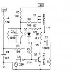
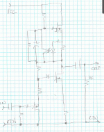
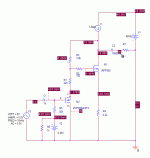
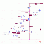
For convenience, the "rippee", Nelson's original GeneSiC design (with one added resistor), and the proposed "ripoff" version replacing the GeneSiC device with a buffered fake SIT. Again, placeholders, as the design has progressed slightly since.
Edit - In fine ripoff tradition, I borrowed the GenSiC schematic from Lazybutt, who posted it in the thread cited previously. As mentioned above- I stole what I liked about it, and changed what I didn't like....
Edit - In fine ripoff tradition, I borrowed the GenSiC schematic from Lazybutt, who posted it in the thread cited previously. As mentioned above- I stole what I liked about it, and changed what I didn't like....
Attachments
Last edited:
This thread will chronicle development of an amp that blatantly rips off the optocoupler-mediated current source...
Ah, you mean "pays flattering tribute to"
I am not sure what the function of R6 is, however if it gets too large there may be a turn-on thump. The time constant of R9 and C2 slows down the turn on of the top CCS so it slows down the time it takes the + side of C3 to rise (charge) to half the rail voltage. I do not by the way see how it can be assured it will rise to half the rail voltage. The gate-Source threshold voltage of Q1 will vary by a few volts from lot to lot (datasheet says -1.5v to -3.5), if you try to adjust R5 to compensate for variation from amp to amp the feedback value will be different and so the gain from amp to amp will be different. You could try doing two loops one AC loop blocked by a cap. and a high resistance pot for the DC control loop. I am not sure if the DC blocking would keep the feedback loop a "Fake SIT".
I give you a lot of credit for building though, I really need to build more.
What I really want to ask is the subjective question, does this topology sound like a true First Watt SIT? Srajan from 6moons attributes a magical "big" sound to the true SIT-1. I suspect SET amps may sound so good with full range drivers because the square law response may cancel distortion as the voice coil starts to move outside of the speakers magnetic poles.
One way to make both sides of a stereo amp the same gain would be to match the bottom side fets, both p and n channel, allowing R6 to be the same for each.
One could also break the ground side of R1 loose and apply a bias voltage to adjust output centering independent of gain. A 9V battery and a pot would be a useful exploration tool in that case...
Taking the design a bit further, one could add a bipolar supply and p-channel differential pair at the input and feed back to it, allowing one to ditch the output caps. This would make the design similar to the "Aleph McSIT", which uses a largish Ixys depletion mode fet for the topside current source.
As for R5, if I add it at all, my inclination would be to set its break point with C2 to 5Hz or below 100 ohms would do nicely.
As for sound, I have not neither heard nor seen a real SIT (even Papa's), but I have been messing with fake SITS (knowingly or not) since 2007, with listenable results.
Last edited:
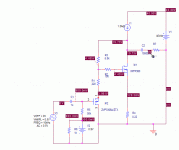
This afternoon, I ran some PSpice simulations on the buffered "Fake SIT" that constitutes the bottom half of this amplifier, fed on top by a simple 1.5A current source.
What I was after was the effect of breaking the ground connection to R1 and adding a bias supply to tweak the output voltage centering independent of the overall gain as set by R5. This works, and I was able to adjust the gain from ~4X to ~12X by juggling R5 and the bias setting, still keeping the output centering at ~1/2 Vcc.. A volt or less does the job, something you could set up using a cheapo yellow-green LED as the voltage reference.
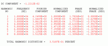
Since I was trying to push up the value of R5 for more gain, a positive bias does it, so no additional bias supply is needed. The consequence of pushing up the gain is less feedback around the output mosfet, hence more distortion, entirely dominated by 2nd and 3rd harmonics.
Next up is developing a rationale for for predicting the gain of the buffered fake SIT.
What I was after was the effect of breaking the ground connection to R1 and adding a bias supply to tweak the output voltage centering independent of the overall gain as set by R5. This works, and I was able to adjust the gain from ~4X to ~12X by juggling R5 and the bias setting, still keeping the output centering at ~1/2 Vcc.. A volt or less does the job, something you could set up using a cheapo yellow-green LED as the voltage reference.
Since I was trying to push up the value of R5 for more gain, a positive bias does it, so no additional bias supply is needed. The consequence of pushing up the gain is less feedback around the output mosfet, hence more distortion, entirely dominated by 2nd and 3rd harmonics.
Next up is developing a rationale for for predicting the gain of the buffered fake SIT.
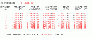
This is what the distortion looks like with a gain of ~6, R3 = 2.2k, Bias V2 = -0.3V. If you push the gain down far enough, you need a negative voltage for bias V2 to get proper centering. I suspect the results will be different for a real IRFP260 and ZVP3306A as compared to the simulation. When I was building the "Aleph McSIT", I had to considerably tweak the values around the fake SIT portion.
At any rate, food for thought as always...
At any rate, food for thought as always...
Attachments
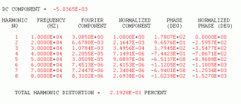
Just for grins, here's the simulation tweaked for a gain of a little over 8, or 18 dB. Since the extra bias needed for centering is positive, no extra supply is required and you can generate the bias from the Vcc supply (though it's a bit wasteful..). I would use an old-school GaAsP red or yellow-green GaP LED as the reference source - quiet, cheap, and pretty. ")
Attachments
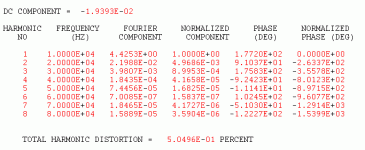
Lowering the impedance of the drive network for the bottom fet lowers the distortion, possibly by increasing the bias current in the p-channel fet as well as decreasing the driving impedance to its gargantuan n-channel sibling. You could possibly be very generous with the bias current in the p-channel, as the voltage across it is small. In this case, the bias current in the p-channel fet is 8.5 mA vs. 4 mA in the previous example . The gain is the same for both.
Attachments
Last edited:
Funny thing -I tried adding a supplemental current source to the source of the p-channel from Vcc, but it did nothing to help the distortion, while lowering the feedback resistors from the n-channel drain to the p-channel source worked well. This time, simpler is better. I'll try lowering the impedance even more tomorrow. Cranking the dissipation on the p-channel up to a staggering 100 mW might work wonders.
- Status
- This old topic is closed. If you want to reopen this topic, contact a moderator using the "Report Post" button.
- Home
- Amplifiers
- Pass Labs
- "Light Touch" Class A Amp