Originally posted by gootee You're welcome. But I don't consider myself an expert at this stuff, anymore (maybe two or three decades ago, I wasn't bad). So I hope that someone else will chime in, to verify (or question) the conclusions et al.
Don't be so modest...I've seen your work at your site, anyone can learn a trick or two from there.
Originally posted by gootee Congratulations on your discrete AD797. And yes! Scott Wurcer! I greatly admire him, too. He's one of those rare guys whom I wish lived next door to me.")
It's to soon for cigar and champagne, I am afraid...but thank you anyway. So far I am done with a layout in Eagle, just buying some extra time to look for mistakes or something that could be improved even further.
Originally posted by gootee With the square waves, remember that the edge-times are what matters, more than the repetition rate ("frequency"). And yes, I would _definitely_ try it with capacitive loads. But be mentally prepared for some "ugliness", at first (just in case
Note, too, that sometimes, even if an amp can drive 1 uF or 2.2 uF OK, and can also drive .001 uF OK, it still might oscillate with a 0.1 uF load (just for example). At any rate, you will probably want to be able to drive a load at the other end of some length of cable (or PCB trace, at the least). And cables (and PCB traces) always have some capacitance. You can look up some common cable capacitances (usually expressed "per foot"), and can probably model them as small capacitors in parallel with your resistive load. At least a few hundred pF or more is probably a reasonable minimum.
I think there is actually a sort-of "standard" for acceptable ringing into a 2.2 uF purely-capacitive (I think) load, for audio amplifiers. I saw it on the web, somewhere, within the last year or so, IIRC. There was something about the percent max overshoot, and something about it dying out within 5 (??) cycles, to within a certain percentage of the initial overshoot. But that's also all assuming a complete amplifier. And a lot would depend on things like the Thiele network (the parallel L and R that that are usually in series with the output, plus the Zobel network(s)). And maybe there would be an R in the forward path, after the amp, but inside the feedback loop, possibly with an L in parallel with the R, which is one way to condition an amp to deal with capacitive loads, IIRC.
I have an RF filter at input and now experimenting with Thiele as well as Zobel network at output...curiously, simulated results indicate better results in step response without Zobel network (100R+100nF) at output...any clue?
I am still not much started in my simulation education, so this observation may be out of place.aparatusonitus said:..curiously, simulated results indicate better results in step response without Zobel network (100R+100nF) at output...any clue?
The model is somewhat simplified and likely does not include for capacitances and inductances in the built unit. As such the sim is unlikely to truly predict the real effect or non effect of the output Thiele network.
Hello All
Thanks Master Gootee help, I have done the simulation, those 2 figures are the result
DZ-Leach close loop gain simluation result
http://img176.imageshack.us/my.php?image=closelp2xm2.jpg
This simulation reslut shown gain reach 0dB around 400KHz
and phase margin is around 80 degree (sorry i forgot to use cursor)
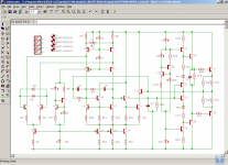
clos-loop gain/phase simulation schematic
http://img526.imageshack.us/my.php?image=closelpcapture1qo5.jpg
This shown the VAC source is in the feedback "base" pin
acout and acin mean Vout and Vin
thanks the friends of DiyAudio help to solve this problem.
but could I use this thread to ask some P-spice simulation question???
like transconductor(Gm) or distortion problem!!
Thanks Master Gootee help, I have done the simulation, those 2 figures are the result
DZ-Leach close loop gain simluation result
http://img176.imageshack.us/my.php?image=closelp2xm2.jpg
This simulation reslut shown gain reach 0dB around 400KHz
and phase margin is around 80 degree (sorry i forgot to use cursor)
clos-loop gain/phase simulation schematic
http://img526.imageshack.us/my.php?image=closelpcapture1qo5.jpg
This shown the VAC source is in the feedback "base" pin
acout and acin mean Vout and Vin
thanks the friends of DiyAudio help to solve this problem.
but could I use this thread to ask some P-spice simulation question???
like transconductor(Gm) or distortion problem!!
mclarenpingu said:Hello All
Thanks Master Gootee help, I have done the simulation, those 2 figures are the result
DZ-Leach close loop gain simluation result
http://img176.imageshack.us/my.php?image=closelp2xm2.jpg
This simulation reslut shown gain reach 0dB around 400KHz
and phase margin is around 80 degree (sorry i forgot to use cursor)
clos-loop gain/phase simulation schematic
http://img526.imageshack.us/my.php?image=closelpcapture1qo5.jpg
This shown the VAC source is in the feedback "base" pin
acout and acin mean Vout and Vin
thanks the friends of DiyAudio help to solve this problem.
but could I use this thread to ask some P-spice simulation question???
like transconductor(Gm) or distortion problem!!
Hi mclarenpingu,
Actually, I'm probably more of a 'Mister' than a 'Master', at my age. But please, feel free to call me Tom. The only person who regularly used the title 'Master', to address me, was one of my grandmothers, mostly during the first half of the second half of the last century.
I guess I'm lucky that my name isn't Bates. ;-)
Anyway, congratulations on getting your phase margin measurement open-loop simulation method to work properly.
Regarding using this thread to ask Pspice questions, etc: I guess you could do that, since it's your thread. But you would probably get more responses if you used a new topic for each question.
Hello Gootee and All master
I still have a problem of this simulation
I use Gootee's diagram (post in No.15)and finish the simulation.
but there still one problem always make me confused very much
" you can insert an AC source just before a high-impedance input"
Yes, I have simulation some difference AC source placement, if I put AC source in the
high impedance node (feedback BJT input side), the result is correct,
but if I put AC source in the output side (Fig. C1, C2, R1 node)
it also can say: make the AC source through whole B circuit(B circuit is feedback B circuit)
contain the resistor of B circuit.
but this will have a wrong simulation result
http://img159.imageshack.us/my.php?image=4395aao7.jpg
This Fig. is copy from Agilent 4395A spectrum analyzer
it tell us put the AC source between the output side and feedback B circuit
I have a question, if we put AC source in the high impedance
the signal did not flow to the feedback resisitor, this is a little stranger
please help me every master!!!!
thanks you very much
have a nice day!!!
- Status
- This old topic is closed. If you want to reopen this topic, contact a moderator using the "Report Post" button.
- Home
- Amplifiers
- Solid State
- Leach150 phase margin problem!!!