Hi.
I was searching for a discrete opamp designs and saw an old
article by W.Marshall Leach about high bandwidth preamp.
In the article he has two designs of a phono preamp and an
output stage. The designs are actually discrete opamps, one
using BJT's at input and the other FET's.
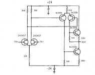
The opamp is designed to work with +-24v.
I ran simulations of the opamp and everything seems ok,
but for use with +-15v it's a bit weak.
Maybe I should add a current source for the LTP, any Ideas?
Help is appreciated...
Thanks,
Udi.
Edit: I used bc550/560 instead of the original 2n5210/5087
The schematics:
I was searching for a discrete opamp designs and saw an old
article by W.Marshall Leach about high bandwidth preamp.
In the article he has two designs of a phono preamp and an
output stage. The designs are actually discrete opamps, one
using BJT's at input and the other FET's.
The opamp is designed to work with +-24v.
I ran simulations of the opamp and everything seems ok,
but for use with +-15v it's a bit weak.
Maybe I should add a current source for the LTP, any Ideas?
Help is appreciated...
Thanks,
Udi.
Edit: I used bc550/560 instead of the original 2n5210/5087
The schematics:
Attachments
Hi,
no or yes?
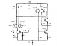
in mk2 the tail current through the ccs forces 1mA through each leg of the ltp.
the 3k6 generates 3v6 and forces 3v across the second LTP tail resistor which in turn creates the bias on the output all ok and r1 is not tied to r2.
In mk1, r1 &r2 both dissipate about half supply voltage. r1 carries twice the current of r2 and for a balanced LTP the relationship is important. So for resistor loading the times 2 relationship is yes.
regards Andrew T.
edit I hope I have the I's & R's the right way round. I cannot see the schematic while typing this reply.
no or yes?
in mk2 the tail current through the ccs forces 1mA through each leg of the ltp.
the 3k6 generates 3v6 and forces 3v across the second LTP tail resistor which in turn creates the bias on the output all ok and r1 is not tied to r2.
In mk1, r1 &r2 both dissipate about half supply voltage. r1 carries twice the current of r2 and for a balanced LTP the relationship is important. So for resistor loading the times 2 relationship is yes.
regards Andrew T.
edit I hope I have the I's & R's the right way round. I cannot see the schematic while typing this reply.
AndrewT said:Hi,
why the different values of second LTP load 1k8 & 1k6?
What is the LED voltage? 470r might be a little low for 2mA.
regards Andrew T.
Hi Andrew,
The different values are like in the original schematic.
when I ran simulation, I found that if both values are equal
than the transistors are not balanced.... though I don't
know why..it seems strange...
the led is 3mm and it's voltage - 1.65, so
I=(1.65-0.65)/470=2.12ma, so that's ok.
Thanks...
Udi.
hi udip,
When using jfet like 2 independant 2N5457 ensure that they are matched because in a real life circuit you will encounter problems if their characteristics (IDSS, yfs, VGSoff, etc) are too different (DC offset, linearisation, etc). On way to compensate is the use of a trim pot between the sources of the jfet.
fab
Hi fab,
I must say that you are correct, I'v just finished building this opamp with no special matching between the fets (just idss), and it worked, but I had something like 5 - 10v offset!!
I guess it's important to match them perfectly...
Anyone knows how to cascode the input fets??
Thanks,
Udi.
I must say that you are correct, I'v just finished building this opamp with no special matching between the fets (just idss), and it worked, but I had something like 5 - 10v offset!!
I guess it's important to match them perfectly...
Anyone knows how to cascode the input fets??
Thanks,
Udi.
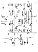
The current sources rely on the voltage across the LEDs in order to provide a constant current. Although LEDs nominally have a constant voltage drop across them, it actually varies slightly with current, so if you used e.g. a resistor in place of T5, variations in supply voltage would yield (small) variations in current out of the current sources. So T5 increases PSRR.udip said:...But why do we need a current source (T5) for a current source
like in this elektor scheamtics??!?!

The reason for the different load resistors in the second LTP is because one of the output transistors is connected common collector and the other one common emitter. They would have different input impedances (resistance) in parallel with the LTP load resistor. The LTP load resistors would have to be selected so the LTP transistors see identical loads. Also each LTP load resistor goes to a different voltage. They both doen't connect to the -24 volt rail. That is probably the primary reason.
Regards,
Ray
Regards,
Ray
It certainly is possible. You can make an op-amp with any output stage you want, as long as it's capable of driving any load you may connect it to.udip said:Is it possible to make an opamp with single-ended output
stage?? (forgive me if it's a stupid question)
Hi !
What do u guys think about my simple discrete opamp??
I'm just starting to learn, so this design may not be perferct...
Also I was aiming for single ended operation...
Will this circuit work in the real world?? I seem to have
a problem with dc offset (Is this normal for single-ended?),
and I guess the open loop gain is a bit low.....
Any suggestions to improve it??
Help will be appreciated...Thanks...
Udi.
Attachments
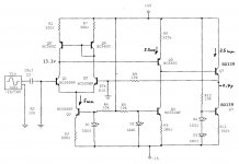
Looks good. The degeneration on Q8/Q6 and Q5 is maybe a bit heavy, and some degeneration on Q1/Q2 might be a good idea. I also don't see any frequency compensation. Is it stable without it? Even if it seems to be, bear it in mind that things are often less stable in real life than in simulations.udip said:...What do u guys think about my simple discrete opamp??.
You'll just have to include some way of adjusting the offset.udip said:...I seem to have a problem with dc offset (Is this normal for single-ended?)...
Open-loop gain doesn't really matter in itself. What matters is the closed-loop performance. If it works, it works.udip said:...and I guess the open loop gain is a bit low....
Pass DIY opamp article
Here you have a direct link to Nelson Pass´DIY opamp aricle:
DIY opamps
udip said:
Anyone knows a good book/article on designing discrete
opamps?? (bias currents, input stages, input impedance,
output stage, se, pp, etc...)
AndrewT said:Doug Self and Nelson Pass both have good websites that show this topic.
Here you have a direct link to Nelson Pass´DIY opamp aricle:
DIY opamps
- Status
- This old topic is closed. If you want to reopen this topic, contact a moderator using the "Report Post" button.
- Home
- Amplifiers
- Solid State
- Leach opamp