I am so glad I don't do automotive electronics anymore. It was a tough way to get a paycheck.I worked closely with Bosch and a bunch of other tier one vendors for 5 years supplying power mosfets for ECU's and ABS breaking. Auto electronics is hugely demanding and the manufacturing quality is superb - non of the suppliers take short cuts.
Alumina substrate is commonly used for hybrid modules. .
For super-low-loss dielectrics for JFET packages, there is alumina, and as well BeO and cubic BN. I probably told the story (yes, I see via Google, in this interminable thread in fact!) of the earnest folk at Lawrence Berkeley Labs who wanted to get rid of the feedback resistor in charge amplifiers, and to facilitate an optoelectronic feedback approach, removed a 2N4416 from its case. They got a wonderful improvement in charge noise and attributed this to the elimination of the high-meg resistor.
Kern and McKenzie at Bell Labs didn't find the Berkeley group's explanation convincing. They repackaged JFETs in low-loss headers and still used a feedback resistor (I recall it was 2Tohm) and got comparable results. They pointed out that it was the lossy borosilicate glass of the normal JFET case that was the culprit. Of course the JFET was at a low temperature for this sort of work.
For years I continued to encounter people who remembered how cool the opto feedback was, and didn't realize that the Berkeley group was mistaken about the primary reason for the noise improvements.
But what does this have to do with audio?
And as Hedley Lamarr asks, Why am I asking you?
Yeah - tough but a fantastic learning environment for me and the teams I worked with. We were the first company in the world to get trench technology auto qualified. It took over a year with B to get it to the point where they were happy to use thrm in volume (100 million a year) in ABS and other stuff. A few years later I went to see IR in California. They told me they never really rated Philips as a MOSFET supplier until we got trench qual'd for auto at B. Big wake up call for them.
However, the respect for that work goes to the 20 odd PhD's we had working on process, packaging and applications not including a few others at the Nat Lab.
However, the respect for that work goes to the 20 odd PhD's we had working on process, packaging and applications not including a few others at the Nat Lab.
Personally, for solid state mainstream audio I would not worry about PCB DF. It's way, way down on the Pareto of things to agonize over. If it is a problem in a specific circuit, I'd posit the designer should question why they are using high resistor values and or why they have hi-Z nodes in their circuit. The worst case I have is 2.5 k which is the 10 k volume pot set to mid position.
Not glass but ceramic: the TDS series Tektronix oscilloscopes attenuators and input stage circuitry. Double sided, thin film deposited resistor (laser adjusted) vias, gold traces, one IC, shortly a piece of jewelry.
Using and doing similar where I am at the moment, cant use any plastic components directly, so we have to do either hermetically sealed hybrids or ceramic modules, near space upper atmosphere stuff so they are neurotic about using plastic components since one failed a few years ago...
A more common way of doing the modules these days is to use a BT epoxy substrate interposter matches the base laminates CTE better than ceramic, cheaper and easier to manufacture... Most BGAs are done this way.
Not audio but the most impressive hybrid I have used is the ford EDIS module. I was a thick film hybrid potted in some sort of jelly protective goop. You could rework through the goop. Never found a reference for what it was.
Impressive because an auto OEM bothered to do that and it was so over engineered that they are almost indestructible. The off road crowd love them for engines that run underwater. And easy to drive from a simple micro. I can only assume that as this was Fords first foray into distributorless ignition they dared not mess it up.
Low pressure moulding probably used a lot in automotive, do a fair bit in this sector mainly the sports side of things... and a lot of modules are encapsulated in low pressure moulded housing, Henkel is a good source of info.
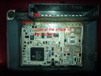
Found a pic of the EDIS hybrid in its goop. I would love to find where to get the goop from as great for DIY automotive stuff. This was around 1983 it was released. I used have a kit car so finding things OEMs had spend $$$ developing to help get you running for a few $ in the junk yards was always fun.
Huge leap of faith from the single coil that went before!
Huge leap of faith from the single coil that went before!
Attachments
I worked closely with Bosch and a bunch of other tier one vendors for 5 years supplying power mosfets for ECU's and ABS breaking. Auto electronics is hugely demanding and the manufacturing quality is superb - non of the suppliers take short cuts.
Alumina substrate is commonly used for hybrid modules. .
We do some ECU stuff more neurotic than some mil/aerospace all ceramic decoupling caps doubled up and placed in pairs with a 90 degree rotation between each one to cater for possible failure mode due to cracking (board flexing) and going short circuit. Not a problem for audio but if you are doing a design that may be exposed to high vibration it is a good safety method to avoid shorts across the power rails.

It would appear that TEK kept its own consul when it came to what substrate material to use for critical locations. Good for them, and I advise anyone to look closely at the FR-4 material that you choose. I think we can be assured that some FR-4 is far worse (even in measurement) than other FR-4 material, so I would recommend being careful. For example, FR-408 , might be a really good choice. I am certainly going to try it.
As I have suggested before look at some of the high thermal conductivity laminates, the extra cooling ability is probably going to be more beneficial than Da...
Arlon 92ML
Ecool-M R15T1 R14T1
The laminate manufacturers will have material spec sheets... for all their laminates.....
Found a pic of the EDIS hybrid in its goop. I would love to find where to get the goop from as great for DIY automotive stuff. This was around 1983 it was released. I used have a kit car so finding things OEMs had spend $$$ developing to help get you running for a few $ in the junk yards was always fun.
Huge leap of faith from the single coil that went before!
I don't see any goop. Is that because it's clear?
If so, the IGBT modules I recently autopsied had the same stuff. It was a layer of gooey clear poured onto the chip/wirebond area, and then they floated a hard clear epoxy on top of that.
They use the clear goop to protect from enviro as well as dampen any vibration. Under hood is vibe sensitive, especially the aluminum wirebonds, and IGBT's are sensitive to lorentz forces on the bond wired during pulse operation.
Might want to ask an IGBT vendor what the goop is.
John
If you look closely you can see it. similar consistency to good pork pie jelly.
Good call. One day will find out as it seems to have many uses for the audiophool worried about vibration.
Um, Bill...while we share a common engineering background, we do not share a common language...
pork pie jelly??

John
edit:
From masterbond:
mastersil 152 looks promising, service temps from -65 to +400, seems good for under the hood.
Supergel 9 looks good as well, but service temps are from -100 to +200F, so may not be good enough for under hood.
Last edited:
Um, Bill...while we share a common engineering background, we do not share a common language...
pork pie jelly??
John
The stuff that oozes out and solidifies, the clear stuff in a good head cheese a most excellent analogy. I've seen the stuff too, I could ask around.
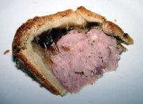
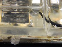
Here's a pic. The block of clear is the hard epoxy overcoat. The lower left "flake" is the goop that oozes out and is sticky to the tough (pardon the technical terminology). That's the stuff we be talkin bout.
This package is a 400 amp IGBT that "blowed up...sir". The base is nickel plated copper, the substrate is direct bond copper on alumina, soldered to the copper base plate.
The black looking thing is one of 4 paralleled IGBT chips. In this particular case, this unit is a quarter bridge IGBT, those black chips were destroyed during manu production test. They start with half bridge devices, and if one side blow up, they cut the wires and sell it as a single leg device with freewheelling diodes. We blowed up the other half. Then I had to determine how we killed it. These particular ones blew up because the unit turned off too quickly. As a result, the periphery of the chips died.
John
Attachments
gelatinous silicone sounds more appealing than head cheese, somehow I try not to eat pure fat, but not sure head cheese would be a great material on our electronics devices!
Not sure of the chemistry behind a silicone that would be self healing if you cut into it to repair the electronic parts underneath, I'm sure that would be something Sy would know about. Sounds like a specialty silicone with very low cross-linking.
Not sure of the chemistry behind a silicone that would be self healing if you cut into it to repair the electronic parts underneath, I'm sure that would be something Sy would know about. Sounds like a specialty silicone with very low cross-linking.
No, not in this case.The 'jelly' or goop is a silicon oil used for heat transfer.
-RNM
The stuff does not flow, there are no ports for fluid motion. It is not used for heat transfer at all. The device relies only on baseplate contact.
The difference between this stuff and the standard glob top is; this stuff is clear, it has a much lower durometer value, and it retains stickyness.
Otoh, CERN is considering the use of coolant flow for one of their IGBT applications. I have cautioned them on that because the device is designed as a bottom directed heat transfer path. Trying to use a laminar flow coolant on the die surface can cause cavitation during heat pulses, which will generate hotspots that the semi chip may not be able to overcome. To increase flow to turbulent to aid in thermal transfer and sweep cavitation bubbles can lead to flexure related wirebond failures.
John
- Status
- Not open for further replies.
- Home
- Member Areas
- The Lounge
- John Curl's Blowtorch preamplifier part II