If your amplifier is stable there is no need for compensation, I only added 4.7pF via a 2.7k resistor in the feedback.
That was enough in my case to calm the problematic 2SC1941, with the rest driver and even with the one of 400MHz I had no problem.
2SC1941 has at 19V Cob below 2pF and the ones I used had an hfe of almost 400.
It is desirable that the outputs have as much gain as possible so as to avoid large currents through the driver and thus increase the number of transistors that can be used for the driver.In my case it is below 10mA and enough for the output to have a collector current of 2A.
My outputs have almost hfe of 180, so they are Y rank as seen on my circuit page before.
Attachments
There isn't any real reason for using high speed power transistors in class A so if it's the gain linearity you want without so many stability concerns, then Onsemi's MJL, NJW21193 or 21194 etc. make more sense for output devices. In any case, don't forget to measure hFE with the power transistors bolted to a heatsink and with normal DC bias current flowing. Isolated measurements with a multimeter or component tester at only a few mA test current are meaningless for class A or even AB power devices.
If your amplifier is stable there is no need for compensation, I only added 4.7pF via a 2.7k resistor in the feedback.
I was actually thinking for your amp, since it needs some compensation. I was just thinking if it could be an improvement in sound or measured performance since some people don't like with having a 'speed up cap' on the feedback from the output. They say it invites HF from the speaker cables etc acting like antennas, better to make the speed up loop 'internal'.
I have no experience in the matter myself.
Except that the more recent types have higher gains, in general, compared with the MJ21194. That should give lower distortion. And it seems possible to stabilise the circuits with a small capacitor if needed.
A multimeter is not ideal to measure the gain of a transistor because it is more often necessary to know the collector current, and multimeters often just provide a base current so that the gain can be read from the Ic value. For matching, you also need Vbe's to be as close as possible, as well as gain, so I use an IC socket for small TO92 devices. For power devices I keep a heatsink with a TO-3 socket to bolt down devices I need to measure, wiring already in place. TO-264 or other devices are less convenient as I don't have a socket for them, but generally manage with small croc clips to the leads.
Not sure how to handle SMD devices as they can be difficult to contact but I have used a small PCB layout with a small spring loaded pin on top, but keeping them in place is sometimes tricky.
Last edited:
A direct output to feedback capacitor is not really a speed up cap - that would apply to a forward path - but a phase correction because with high speed output transistors, you have three stages with more or less the same frequency response, which is certainly potentially less stable than an amp with slower devices. The amp may then depend on the driver transistor as much as either of the input or output stages, and that could be sensitive to Cjc, hence variable performance between builds when different drivers might be used.
One slower stage can provide better inherent stability.
The compensation capacitor can be routed from the driver collector instead of the output. In circuits where I have used a connection from the output I've added a CR/ LR network to prevent HF pickup.Some people don't like all those mods on a JLH.
Update Circuit Q3 and Q4
Hi, altus fidelitas.
I did an update on my circuit.
I replaced the Q3 and Q4 transistors.
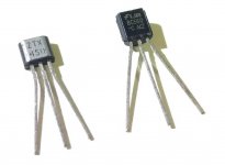
Q3 (before: 2N1711, now: ZTX450).
Q4 (before: 2N2907, now: BC560).
I'm still doing some tests.
Thanks for the tips guys!
You could consider replacing 2N1711 with a ZTX450. It has better gain and linearity than both the BD139 and 2N1711. I used it in my recent build and it sounds good.
Some concerns that it comes in a tiny E-Line package, but its specs add up and they were not at all warm when I measured them.
I replaced the Q4 (2N2907) with a BC560, a low noise signal transistor. But original ones are difficult to get these days with lots of fakes around. Apparently BC850 shares the same die as the BC560 but its in a SMD package.
Hi, altus fidelitas.
I did an update on my circuit.
I replaced the Q3 and Q4 transistors.
Q3 (before: 2N1711, now: ZTX450).
Q4 (before: 2N2907, now: BC560).
I'm still doing some tests.
Thanks for the tips guys!
Attachments
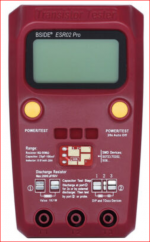
The attached image is of an unusual Chinese component tester adapted for SMDs but I can't recommend it because the display is awful, it's now way overpriced, a 9V battery is required and it does no more that any other ATMEL 328 based tester. However, I think its SMD test feature is more or less along the lines of yours and it has gold plating on the contact pads which does improve the consistency of measurements a little in my estimation.Not sure how to handle SMD devices as they can be difficult to contact but I have used a small PCB layout with a small spring loaded pin on top, but keeping them in place is sometimes tricky..
A clip that keeps the little devils in firm contact is probably essential but not if it can slip and launch them to oblivion instead. It wouldn't be all that difficult to copy the jig essentials and adapt it to your existing instruments with some gold plated copper foil pads on a board. Then add a mask or close fitting jig cut from sheet plastic to keep any particular outline SMD aligned correctly on the contact pads. The pads could simply couple to your own preferred semi testing device via PCB pins, header and 3 core ribbon or whatever suits your purpose.
Attachments
Gold plated leads are almost mandatory for reliable contacting.
Soldered pads are uneven, if done with a standard iron, so usually I just use plain copper pads but clean the tracks before measuring. Carefully. as the tracks are small and fragile.
Good idea to make a perspex jig to hold them in place.
Soldered pads are uneven, if done with a standard iron, so usually I just use plain copper pads but clean the tracks before measuring. Carefully. as the tracks are small and fragile.
Good idea to make a perspex jig to hold them in place.
An externally hosted image should be here but it was not working when we last tested it.
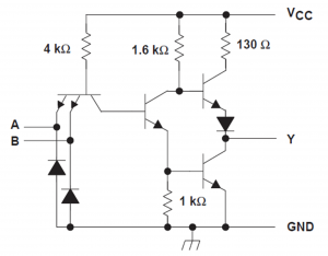
Part of the main TTL (7400) circuit. Phase splitter stage and totem pole output stage (1965).
It was originally based on circuitry for vacuum tube.
Here is a US patent for a telephone line amplifier (a circuit with 4 transistors - a complete match).
Hood referred to Williams' amplifier.
https://www.electronics-tutorials.ws/amplifier/phase-splitter.html
Last edited:
My 2SC5200s have arrived. 4 out of 5 have very healthy gain (150-170 range). The 5th one is way down at 58. Good thing I only need 4. ")
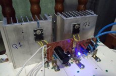
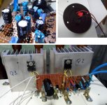
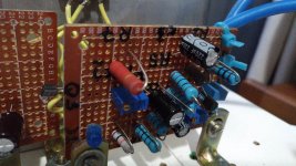
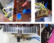
I'll be continuing to plan the cooling solution and will probably start building the circuits soon. I am cheating by using a PCB kit from ebay.
I'll be continuing to plan the cooling solution and will probably start building the circuits soon. I am cheating by using a PCB kit from ebay.
An externally hosted image should be here but it was not working when we last tested it.
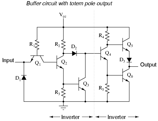
Totem PolesHi all! I'm interested who and when invented a 3-transistor combination = JLH without first transistor. Smb help?
A very popular output design is nick named the "Totem Pole" output stage. This is a "stack" of transistors of the same polarity, usually PNP germanium devices in the '50s and '60s, and later NPN and silicon devices came along in the '60s and '70s.
Solid State History - davidmorrinoldsite
I remember, but I can't find it. Linear amplifier with PNP transistors. Three-stage: entrance, phase splitter and push pull totem pole. The signal is applied to the emitter of the first transistor (like the NFB).
Japanese firms waxed lyrical about their "SEPP-OTL" circuitry. I knew OTL stood for Output Transformer-Less, but at the time I hadn't seen that SEPP was single ended push pull.
Single-ended Push-Pull - UK Vintage Radio Repair and Restoration Discussion Forum
PNP stages require the collector load negative to the emitter.
This example on Douglas Selfs site by Tobey and Dinsdale (1961) is typical.
http://www.douglas-self.com/ampins/wwarchive/Tobey & Dinsdale power amp Nov61 p2.jpg
The SEPP circuit refers only to the particular circuit by Peterson/Sinclair, and always has. It consists of three valves, one of which acts as a phase inverter. This is the quintessential SEPP:
https://patentimages.storage.googlea...S2802907-0.png
Last edited:
United States Patent Office 3,320,543 Patented May 16, 1967
Filed Mar 25, 1964, SerNo.354,635
A. HOPENGARTEN ETAL 3,320,543
TRANSISTORIZED PUSH-PULL AMPLIFIER CIRCUIT
UTILIZING POSITIVE FEEDBACK Filed March 25, 1964
References Cited by the Examiner
UNITED STATES PATENTS
2,802,907 8/1957 Peterson et al. ------ 330-81
2,929,026 3/1960 Walker ------------- 330-70
FOREIGN PATENTS
213,957 3/1961 Austria.
OTHER REFERENCES
Aronson et al.: "Transistor Audio Frequency Ampli fier," RCA TN No. 36, rec'd in Patent Office Aug. 9, 1957, 1 sheet, 330-14.
“Output Transformerless Amplifiers,” Wireless World, February 1957, pages 58-62, copy in Scientific Library or
330-70.
Last edited:
I need to verify some info/math re: dissipation.
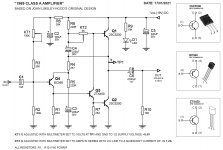
JLH states the following in his original (1969) article:
The voltages and currents displayed in "Table 1" of the article all work out to be about 32-34 watts.
17V * 2.0A = 34W
27V * 1.2A = 32.4W
36V * 0.9A = 32.4W
Therefore, the total power dissipation is divided across the 2 output transistors, with each output transistor dissipating ~17W. Correct?
JLH states the following in his original (1969) article:
Since the supply voltages and output currents involved lead to dissipations in the order of 17 watts in each output transistor
The voltages and currents displayed in "Table 1" of the article all work out to be about 32-34 watts.
17V * 2.0A = 34W
27V * 1.2A = 32.4W
36V * 0.9A = 32.4W
Therefore, the total power dissipation is divided across the 2 output transistors, with each output transistor dissipating ~17W. Correct?
- Home
- Amplifiers
- Solid State
- JLH 10 Watt class A amplifier