Hi Wahab,
I will try your mod. Can I use 2SK117GR for Q4?
I only have a few K170BL but I have got a bunch of cheaper Toshiba 2SK117GR with Idss ~ 6mA.
Cheers, Stanley
Hi , Stanley
Not sure but it should do it .
Will do a sim, though..
cheers,
I like the idea of running a .wav file through the simulator, but I doubt it will be accurate since there is not real-time thermal simulation, unless manually implemented. And even then it can only be crude unless you create a discrete version of the component model with added support.
- keantoken
- keantoken
Thanks Hugh,
I will try that with a 15pF ceramic cap as I don't think I have the 15pF silver mica.
Cheers, Stanley
Hello
If you don't have silver mica, use a NPO type ceramic cap, they are much better than the standard ceramic cap.
Bye
Gaetan
With +/-50 Volt supply.
Two pair HEXFET IRFP240/9240 and cascoded JFETs.
IRF610/9610 for VAS.
100 Watt into 8 Ohm with low distortion.
Hello LineUp!
I want to follow this scheme because I now have all the parts fit this scheme. JFETs 2SK170BL except that I do not have, but I have 2SK30A JFETs can I change K30A K170 with it?
I like this circuit! because it matches the speakers have low sensitivity and 4 ohm impedance only for me.
if I need to change any component or value in this circuit?
and then the circuit has good activity and stability after change it JFETs ?
Thank you much!
The only mods i made was to increase the values of the feedback
resistors, as their original values were too low for some obvious reasons,
that allow to get rid of an eventual ugly lead comp. cap and replacing it by
a well more stability enhancing lag cap compensation.
I wonder why you call "lead comp" ugly for me it is the most desirable method becuase it brings stability without sacrificing OLG and is therefore beautiful
")
By choosing the lag cap you are loosing mid & treble OLG which will diminish mid & treble resolution.
For me it is much more satisfactory ( for the sound ) to leave OLG intact and and add compensation direct from the VAS to the i/p Jfet source.
As Hugh states sometimes a bit of both are required but, if designed carefully they perform different actions that operate at different frequencies.
When you add the CCS as the i/p FET drain load on this design you do indeed a miller cap but I would advice keeping it as small as possible and using the lead compensation ( cap from VAS to i/p Jfet source ) to make the amp stable with awkward loads.
With the design swordfishy has settled on, a miller cap is not required and that for me is the one of the best features of it and infact with simple loads no compensation is required at all which is amazing but the amp will be a bit more stable and probably sound a bit better with some ( lead ) compensation added.
Last edited:
I am assuming that lag compensation is having the miller cap from the VAS output directly to the negative side of the comparator (in this case the source of the Jfet(s)).
In this case lag compensation will actually increase OLG, but decrease amplifier gain at the same frequency. Lag compensation is tempting always because it does not cause any extra load on the preceding stages, but most often it doesn't work because there are positive feedback loops in other areas of the amplifier. Lead compensation (miller cap right at the VAS) carpet-bombs most of the issues that can occur there, unless you have fancy cascodes or something exotic with major parasitic feedback paths. Often an RC snubber in the right place can work like magic.
- keantoken
In the schematics here:
http://www.diyaudio.com/forums/soli...as-lateral-output-perfect-18.html#post2600326
Some lag compensation might be appropriate to make up for the extra current the Jfet must provide for the miller cap.
Also, you could always experiment with TMC, which would have less of a performance drop than lead comp I think.
- keantoken
I think we're getting our lead & lag terminology muddled up.
wahab seems to be calling a miller cap "lag compensation" and a cap from VAS to Jfet source "lead compensation"
To avoid confusion, can we agree on this terminology or can some enlightened soul tell us a more standard terminology ?
mike
wahab seems to be calling a miller cap "lag compensation" and a cap from VAS to Jfet source "lead compensation"
To avoid confusion, can we agree on this terminology or can some enlightened soul tell us a more standard terminology ?
mike
Miller cap = Lag Compensation, local feedback from output of VAS to input of VAS (drain/gate, or collector/base), the conventional way of compensating an amp so that loop gain is just below unity at the upper pole frequency when negative feedback turns positive.
Phase lead = JLH technique (and others) of straddling the VAS output and the fb inverting node with a small cap. This is interstage rather than local compensation and it improves the amplifier's tolerance of difficult loads.
Both techniques, and TMC (OS, you there?) have profound influence on amp stability, and curiously, on the sonic presentation of the amplifier.
Hugh
Kean,
You can call it whatever you think is best, but it's a good idea to use the accepted terms in the literature, which are lag compensation, sometimes called Miller compensation, and phase lead, which I've not seen described any other way.
But, have a look at the literature around this component to be sure I'm right!
Hugh
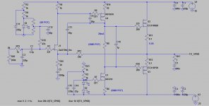
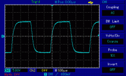
Taking it to the next level...200kHz
Hi all,
Well the long weekend is here and I've been playing around again.
I have taken fetzilla to new levels, though not with any particularly innovative modifications, just a little tweaking.
Please see attached schematic and oscillogram.
I have added:
1) An LED + FET based VAS CCS - simpler, faster and more latch up resistant thn the BJT verson.
2) A little miller compensation.
3) Reduced VAS degeneration. to increase OLG.
4) Increased global feedback.
5) Increased feedback capacitor.
6) Added extra filtering for LED voltage sources, after careful modelling.
The result? The most stable, cleanest and fastest fetzilla yet.
Can it do a 20kHz square wave? Stuff that, let's try 200kHz shall we?
DC offset is the most stable of all the designs I've built so far too, though I'm yet to investigate turn on thump....
Did I mention it sounds pretty good too?
Attachments
Hi,
the J-FET grounded source amplifier converts input voltage signals into current signals with excellent precision. However, the grounded source amplifier amplifies both current and voltage, which is unadvantageous from a linearity point of view. A low load impedance reduces the very high output impedance of the J-FET grounded source amplifier and the voltage gain¤. A load impedance that approaches zero coincides with the requirement for linear current transfer. The grounded base amplifier provides a low load impedance and its overall properties make it superior to other topologies for voltage amplification. The differentiated current and voltage amplification is an important achievement of the J-FET / grounded base amplifier compound (due to nearly unity voltage and current gain respectively).
¤This implies a reduction of Gm, which is part of the voltage gain formula unlike in the case of bipolar transistors, showing a fundamental difference. The lack of relationship between current and voltage gain is one of the numerous causes of grounded emitter amplifier nonlinearity.
For linear function the intrinsic impedance of any voltage source must be near zero.
I think he intends to characterize the issues we grapple with in using a MOSFET VAS in a concise and logical manner so that we may understand better the issues and formulate a better solution.
What he says seems to indicate that cascoding the VAS would be a good option? The terminology is confusing to me but I think I understand. I think he's pretty much discussing Early affect for MOSFETs.
- keantoken
What he says seems to indicate that cascoding the VAS would be a good option? The terminology is confusing to me but I think I understand. I think he's pretty much discussing Early affect for MOSFETs.
- keantoken
There are countless, numerous ways to complicate an amplifier.
Until you have 20, 50 or 100 transistors.
I have seen some from keantoken, too. You can no longer see the light from every improvement. And cascode.
Nelson Pass is a bit better. He uses few devices mostly.
And his projects are very popular and easy to understand.
Fetzilla uses 4 Transistors.
And 2 current sources with a couple of more. And supply trafo 2x18VAC
And this is the way I will keep it.
Because I know most of us like the basic clean circuit.
Regards
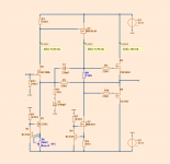
Here is a typical Fetzilla circuit for minimal harmonics distortion:
Until you have 20, 50 or 100 transistors.
I have seen some from keantoken, too. You can no longer see the light from every improvement. And cascode.
Nelson Pass is a bit better. He uses few devices mostly.
And his projects are very popular and easy to understand.
Fetzilla uses 4 Transistors.
And 2 current sources with a couple of more. And supply trafo 2x18VAC
And this is the way I will keep it.
Because I know most of us like the basic clean circuit.
Regards
Here is a typical Fetzilla circuit for minimal harmonics distortion:
Attachments
Last edited:
Lineup,
You are the father of this circuit, and for that we hold you and your inspiration in high regard. Thank you, mate, it's a great conception and since you and I like simplicity, this one is a pearler.
SWF,
You are the only guy here who is listening carefully and can say with authority how it sounds through your above average ear. This is important to me, and a clincher in the deal. From my 15 years designing, building and listening, I can tell you the relationship between measured specs and subjective listening is, well, specious at best.
Your square wave is exceptional for 200KHz, and shows the exact profile of a single ended voltage amplification stage.
I feel your miller compensation could be reduce just a smidgin, perhaps to 36pF. This is important to sound quality, BTW.
Shall I amend the pcb layout? I would suggest that parts availabity is important, and the IRF610 is hard to find in Oz, would you consider using a bipolar transistor here? And the other issue is the feedback network, would you consider making the shunt resistor 100R, designing around that, so that you can reduce the fb shunt cap from 2,200uF down to say 470uF, a more practical size, which might actually improve the switch on thump?
Aside from that, Bravo!!
Hugh
Last edited:
There are countless, numerous ways to complicate an amplifier.
Until you have 20, 50 or 100 transistors.
Fetzilla uses 4 Transistors.
And 2 current sources with a couple of more. And supply trafo 2x18VAC
That s 8 transistors...
A grand total of 20 is way enough to improve the perfs by quite a big margin
while cost would not be much higher.
Attachments
mikelm,
what I`m saying is that the input stage should composed of a J-FET / grounded base cascode, if an additional voltage amplifier stage is desirable it also should be a grounded base amplifier (its emitter directly coupled to the cascode collector, no intermediate grounded collector amplifier and no intermediate grounded emitter amplifier as proposed by some authors).
what I`m saying is that the input stage should composed of a J-FET / grounded base cascode, if an additional voltage amplifier stage is desirable it also should be a grounded base amplifier (its emitter directly coupled to the cascode collector, no intermediate grounded collector amplifier and no intermediate grounded emitter amplifier as proposed by some authors).
- Status
- This old topic is closed. If you want to reopen this topic, contact a moderator using the "Report Post" button.
- Home
- Amplifiers
- Solid State
- JFET input, MOSFET VAS, LATERAL output = Perfect!!