Hi ,
I am given an old amplifier, schematic is not available so I draw output stage from the circuit. I have checked many times to be sure of it. See attached scan.
The amp is singing but its output arrangement puzzles me. Is this output arrangement correct and can perform well? I never see this arrangement before .
.
I am given an old amplifier, schematic is not available so I draw output stage from the circuit. I have checked many times to be sure of it. See attached scan.
The amp is singing but its output arrangement puzzles me. Is this output arrangement correct and can perform well? I never see this arrangement before
.Attachments
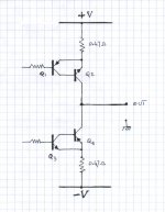
It could be correct, although rather unusual. You appear to have two complementary pairs, but used in common emitter mode rather than emitter follower mode. I assume the two bases Q1 and Q3 are not connected essentially to the same point apart from a Vbe multiplier for bias, but instead have separate drives at potentials near the two supply rails.
Are you sure you haven't got them upside down? i.e. the output connects to the junction of the two 0.47 resistors?
The arrangement you have drawn would have high output impedance, but this could be reduced via global negative feedback.
Are you sure you haven't got them upside down? i.e. the output connects to the junction of the two 0.47 resistors?
The arrangement you have drawn would have high output impedance, but this could be reduced via global negative feedback.
Hi,
The amp is singing but I am not happy with the sound (too harsh, lack of dynamic, sound seems restrained). That 's why I decided to look at the schematic.
I was surprised to see this strange output arrangement, I have checked many times I am pretty sure that I did not make mistake on my drawing. I do not know how can work Q2 and Q4 they are polarized backward right? Can it be a mistake during production? They swapped Q2 and Q4 may be? My first idea was to swap Q2 and Q4 but I changed my mind to post for help.
- 0.47R resistors are in the supply lines and ouput is as in my drawing,
- I have checked also for the NPN and PNP output (Q2, Q4) they are as in my drawing,
I will check again, tomorrow I will also post a more complete schematic.
Thanks for your replies,
Yes, it is wrong - I didn't look closely enough at it. Q2 and Q4 have emitter and collector mixed up. With this corrected it is then a strange circuit, rather than a wrong circuit.
My guess is that this is really a standard complementary feedback pair output, but the OP has got confused somehow. Seeing the previous stage which drives it would confirm this: VAS plus Vbe multiplier says this is a conventional CFP, separate drivers fed from an earlier phase splitter would suggest that it is not a CFP.
My guess is that this is really a standard complementary feedback pair output, but the OP has got confused somehow. Seeing the previous stage which drives it would confirm this: VAS plus Vbe multiplier says this is a conventional CFP, separate drivers fed from an earlier phase splitter would suggest that it is not a CFP.
yes, it works, it is the common emitter output stage requiring a driver stage that uses current through a resistor to the supply rail to control the CFP.
OOPs,
I hold this until I see the corrected schematic.
(The big difference is that the output stage uses two transistors in Baxandall Super Pair arrangement)
OOPs,
I hold this until I see the corrected schematic.
(The big difference is that the output stage uses two transistors in Baxandall Super Pair arrangement)
It looks to me like the Hiraga amp, its the only amp I know of that uses this arangement, it is strange you say the sound is bad as builders of the hiraga are very pleased with their amps saying it sounds very tube like. Maybe in your case something is wrong or its a different amp. Look up threads here about these amps, theyre called hiraga 8w monster amp and hiraga super class A amp, the builders might be able to give some good advice.
Hi everybody,
Here are additionnal info for the output stage. I draw this morning. I have also checked if I made a mistake regarding Q2 and Q4 wiring, I confirm what is in my drawing.
I am waiting for your comments before I decided wether I modified the wiring of Q2 and Q4 on the PCB or not (swap Emitter and Collector). The amp is old I suppose that output transistors are no more in production I don't want to smoke them.
For sakis & homemodder,
I have searched for the schematic more than 6 months no use.
This output arrangement is similar to the Hiraga well known amp except for Q2 and Q4 wiring. Obviously there is problem but
what puzzles me is that amp is singing !
Attachments
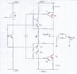
It can't possibly work correctly as drawn because Q2 and Q4 have no base current so at most will act like diodes. This means that the output is being produced by the drivers Q1 and Q3, with the base-collector junction of Q2/4 being forward biassed. With some global NFB it could produce sounds, but output power would be limited as presumably the drivers can't generate enough current.
Just seen your new drawing. That would make sense if Q2 and Q4 had emitter-collector swapped over, to make two complementary pairs with Q1 and Q3.
You can think of this output as a super-complementary pair. Take a complementary pair and add a third BJT to the second to make another complementary pair at the output. Then add a fourth BJT in cascode with the first BJT. The result is what you should have. The third BJT adds current drive capability. The fourth BJT improves power supply rejection and reduces Miller effect.
You can think of this output as a super-complementary pair. Take a complementary pair and add a third BJT to the second to make another complementary pair at the output. Then add a fourth BJT in cascode with the first BJT. The result is what you should have. The third BJT adds current drive capability. The fourth BJT improves power supply rejection and reduces Miller effect.
From your replies you all think that this ouput arrangement cannot work properly. This is also my opinion.
I try to guess what was the mistake during production or this amp was serviced by someone who replaced output devices with wrong pin out?
Tomorrow I will swap over Q2 & Q4 Emitter and Collector of one channel to see what happen and will let you know. Thank you all for spending your time replying to my post.
For Andrew T:
Q1=TIP42C - Q2=BD249C - Q3=TIP41C - Q4=BD250C
Quite common devices more than 10 years back
 No, pin out order for BD249/BD250 is bec
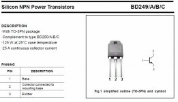
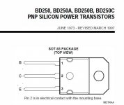
Pin order of BD249/250 is always BCE, with collector (middle leg) connected to case. I have seen literally tens of thousands of these from who knows how many manufacturers and it's always and without fail, BCE, reason being the silicon chip (=substrate) is bonded to the case, and the substrate is always collector due to the required doping. The only part in a TO3P-like case that does not follow this tule that i am aware of, are lateral MOSFETs from hitachi (K1058/J162) which have the substrate, and thus the middle pin and case, connected to the source, rather to the drain which would be the MOSFET equivalent of a BJT collector. In fact, this fact is used to identify fakes of said lateral MOSFETs...
This would mean your amp has a classic common emitter coplementary darlington pair output. It's in fact a current feedback output stage with gain. These can be quite tricky as their open loop gain depends heavily on the load.
This would mean your amp has a classic common emitter coplementary darlington pair output. It's in fact a current feedback output stage with gain. These can be quite tricky as their open loop gain depends heavily on the load.
- Status
- This old topic is closed. If you want to reopen this topic, contact a moderator using the "Report Post" button.
- Home
- Amplifiers
- Solid State
- Is this output arrangement OK?