Q6 and Q7 are emitter coupled pair without a register, which has a large gain and is driven by digital logic. So, their analog response is very limited period only at the transition of V(n008) and V(n009), almost 1 nano-sec. Except for that time, they are on or off, don't act as an analog device. I think they can't be a mixer.
Actually that is exactly how single-balanced transistor mixers are normally made: a differential pair is driven so hard by the LO that it acts as a switch and the RF is superimposed on the tail current.
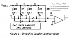
In any case, any type of DAC multiplies its (dimensionless) digital input signal with a voltage or current reference to produce an output voltage or current and therefore acts as a mixer between the digital code and the reference.
My SIM uses ideal inputs V(n008) and V(n009) which comes from FPGA. But almost every output of a digital circuit has the different tplh and tphl. It's practically impossible to have an ideal differential output like SIM. FPGA has internal PLL with being capable of phase adjust by 30 pico-sec step. You can utilize this function to cancel the difference between tplh and tphl. If this adjustment is out of range, SNR becomes far less than with adjustment. 1 nano sec difference usually causes more than 10db degradation of SNR.
As long as I have tested, the most dominating factor to degrade SNR of 1bit DSM is the difference between tplh and tphl. You must adjust this as possible as you can. Multi-bit DSM is free of this problem because they treat an input as a digital one, on the other hand, 1 bit DSM treats an input as an analog one.
I think you could solve that with a return-to-zero DAC, but we had that discussion before.
The constant current source of a breadboard is like attached. SIM is mainly for verification of collector voltage, how fast they can swing. So I use a simple CCS. A bypass condenser crossing R9 is also necessary on a real PCB. Crosstalk from base to a collector is probably neglectable. Because of noise on DSD+ or DSD- are relatively low and R2 and R5 are low compared with base-collector capacitance. The attached pic includes floating capacitances of C5 and C6. With 3pF capacitance, collector voltage is almost same as the real one.
About 3 pF of collector-base capacitance with 150 ohm gives you a cut-off of about 350 MHz, so 17500 times suppression at 20 kHz, so 35 mV of audio-frequency rubbish on the FPGA outputs would result in at most 2 uV on the outputs, which then largely gets cancelled because it is mostly common mode.
You are right, crosstalk through the base-collector capacitance will be negligible.
I partially agree with you about a mixer. It's correct every DACs are multiplying between the reference and the input signal like the attached pic. But the input of a DAC is digital code. The multiplying is between the analog reference and the digital input. An RF mixer such as a superheterodyne is done by two analog inputs.
But you need to consider another "mixer" effect for a multiplying DAC. It's crosstalk from digital input to the reference and analog output. When I think about this type of "mixer," I can remember some cases which had a chance caused by "mixer." I wrote before crosstalk from base to collector could be neglectable. Some are so, and others are not so. This is one factor of degrading SNR, sometimes inherent to a DAC chip and inherent to a PCB, IMHO.
But you need to consider another "mixer" effect for a multiplying DAC. It's crosstalk from digital input to the reference and analog output. When I think about this type of "mixer," I can remember some cases which had a chance caused by "mixer." I wrote before crosstalk from base to collector could be neglectable. Some are so, and others are not so. This is one factor of degrading SNR, sometimes inherent to a DAC chip and inherent to a PCB, IMHO.
Attachments
Crosstalk from the sigma-delta modulate to the reference and to the clock is indeed a problem. It is the main reason why I went from a point-to-point wired version to a four-layer board for my valve DAC; on the point-to-point wired version, simply touching the insulating jacket of a thin coaxial cable that carried the sigma-delta modulate was enough to increase the noise floor by 10 dB or so. I now have all digital stuff on the bottom side, all analogue and mixed-signal circuitry on the top side and use the inner layers as shields and as signal return paths.
Your valve DAC is a fascinating approach.") I think PCB layout is more dominating than a DAC chip. Modern DACs have excellent performance which can be achieved only in the best circumstances. PCB layout and power supply are important. PCB layout usually has less attention than power.
I think PCB layout is more dominating than a DAC chip. Modern DACs have excellent performance which can be achieved only in the best circumstances. PCB layout and power supply are important. PCB layout usually has less attention than power.
I also use four-layer PCB but has another layer structure as you. Almost every part except for bypass capacitors are on the top layer. Analog signals are also on the top layer. The remaining area of the top is the ground plane for a shield.Digital signals are the inner layer(L2). The ground plane is the inner layer(L3). Digital signals are almost sandwiched between the top side ground plane and inner ground plane(L3). The bottom side is power.
My intention is a decrease of radiation noise from digital signals. Inner layer digital signals are less radiative. This is the only attempt for an audio system. This requires more vias than a usual layout. In some applications, many vias cause problems. This is the good layout for high SNR application as long as I have experienced.
For example, If you want -120dBFS(1kHz) signal for an ADC, you have two choices, one is the direct output of -120dBFS from DAC(oscillator), the other is -80dB output from DAC and 40dB ATT in front of an ADC. You can get more accurate -120dBFS with the later. But radiation from digital signals of the ADC sometimes decreases SNR. Inner layer digital signals are less radiative than top side one. My ADC(18 bit) with this PCB structure outputs residual noise only when the input is -120dBFS.
An analog attenuator is not simple. It can't divide the signal correctly in an ordinary condition. Mixed-signal circuitry often produces an unexpected spectrum. That's why I don't use an analog attenuator. It depends on circumstances.
BTW, do you have a photo of your valve DAC? I have less experience with a valve. I made a preamplifier with ECC83 or EF86 forty years ago. Now I'm a silicon people.
I think PCB layout is more dominating than a DAC chip. Modern DACs have excellent performance which can be achieved only in the best circumstances. PCB layout and power supply are important. PCB layout usually has less attention than power.I also use four-layer PCB but has another layer structure as you. Almost every part except for bypass capacitors are on the top layer. Analog signals are also on the top layer. The remaining area of the top is the ground plane for a shield.Digital signals are the inner layer(L2). The ground plane is the inner layer(L3). Digital signals are almost sandwiched between the top side ground plane and inner ground plane(L3). The bottom side is power.
My intention is a decrease of radiation noise from digital signals. Inner layer digital signals are less radiative. This is the only attempt for an audio system. This requires more vias than a usual layout. In some applications, many vias cause problems. This is the good layout for high SNR application as long as I have experienced.
For example, If you want -120dBFS(1kHz) signal for an ADC, you have two choices, one is the direct output of -120dBFS from DAC(oscillator), the other is -80dB output from DAC and 40dB ATT in front of an ADC. You can get more accurate -120dBFS with the later. But radiation from digital signals of the ADC sometimes decreases SNR. Inner layer digital signals are less radiative than top side one. My ADC(18 bit) with this PCB structure outputs residual noise only when the input is -120dBFS.
An analog attenuator is not simple. It can't divide the signal correctly in an ordinary condition. Mixed-signal circuitry often produces an unexpected spectrum. That's why I don't use an analog attenuator. It depends on circumstances.
BTW, do you have a photo of your valve DAC? I have less experience with a valve. I made a preamplifier with ECC83 or EF86 forty years ago.
Now I'm a silicon people.Attachments
Nice board! I posted some photos of my DAC here:
http://www.diyaudio.com/forums/digital-line-level/166807-dac-gallery-24.html#post5065812
http://www.diyaudio.com/forums/digital-line-level/166807-dac-gallery-24.html#post5065812
and the enclosure is being inspected here:
http://www.diyaudio.com/forums/the-lounge/302478-audiophile-cat-6.html#post5016100
http://www.diyaudio.com/forums/the-lounge/302478-audiophile-cat-6.html#post5016100
Hi, I finally understand what you mean. I found a discrete DSM DAC DSC1 made by Signalyst. It uses 32 registers to implement 32taps sinc filter for removal of HF noise. It makes sense. I have never thought about this method. But this is the similar way of pcm1792 which has 64taps FIR filter for DSD. That was a blind spot for me.
As long as I know so far, those who want to convert DSD to analog signal uses simple LPF without a series registers. I also tried in the same way. It didn't work well as I wrote before. If you use such a method, glitch problem is not so critical than a simple LPF.
Have you ever measured the circuit which you posted? I have found several data about DSC1. I don't know what performance it has because accurate values depend on measurement circumstance. The exclusive input to DSD isn't so inconvenient. I don't know why this is less attractive than a discrete multi-bit.
I have measured the circuit of post #5 now. I first found that the common-mode loop was oscillating; shorting the 470 pF capacitor (C11) and putting 15 pF between the negative input and the output of the OPA134 (U3) solved that.
After this fix (and after solving some other minor issues, mostly related to poor soldering), I measured a ratio between maximum signal and A-weighted noise of 97.83 dB.
The accuracy of the measurement is a bit dubious. I first record the signal, the noise and the noise with the DAC switched off with a Fostex FR2LE field memory recorder and then post process everything with a computer. The difference between the noise with DAC on and DAC off was only 1.7 dB; the noise floor of the field memory recorder was higher than that of the DAC I tried to measure.
Last edited:
Very interesting. Many people design their DAC, but few do their ADC. A good ADC can improve the performance of a DAC because a DAC and ADC are related matter. SNR of my ADC is now 113dB. It means max SNR of my DAC is also 113dB SNR. Even if my DAC has 113db SNR, measured data by ADC is square root sum of them; 113-3=110dB. If you get the measured data of 113db, SNR of the DAC must be below 113 by 10dB. Thus, you need to compensate the measured data for accurate value.That's why I 'm now designing my new ADC which has 120dB SNR. This is already beyond listening purpose, but for me very interesting to develop. My implementation of DSM DAC into FPGA is also for this project. DSM DAC is originally for measurement purpose but can be another solution for listening purpose. A DAC and ADC are an inseparable partner.
My sigma-delta modulator has three modes: seventh-order chaotic, fifth-order with embedded pulse width modulator with a factor of four ratio between PWM clock and quantizer clock and fifth order with embedded pulse width modulator with a factor of eight ratio between PWM clock and quantizer clock.
With my valve DAC the PWM8 mode clearly has the smallest in-band noise, but with the (modified) circuit of post #5 it hardly makes any difference. The in-band noise floors are nearly the same for all modes:
PWM4: -97.83 dB(A)
chaos: -97.06 dB(A)
PWM4 (repeated measurement): -97.44 dB(A)
PWM8: -98.32 dB(A)
The out of band noise is different, as expected:
chaos: about 1.3 mV RMS
PWM4: about 2 mV RMS
PWM8: about 6.7 mV RMS
The out-of-band values are estimated by looking at the quasi peak-peak noise with an oscilloscope and assuming that the RMS value is about a sixth of the quasi peak-peak value. The maximum signal level is about 1.96 V RMS.
- Status
- This old topic is closed. If you want to reopen this topic, contact a moderator using the "Report Post" button.
- Home
- Source & Line
- Digital Line Level
- Is DSD signed or unsigned?