.
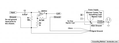
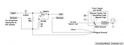
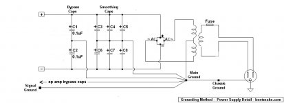
This is my understanding of the grounding method recommended by Douglas Self, the engineering department at Texas International, and others. If I've misinterpreted anybody I'd be very glad to be corrected by them.
This method is not as complicated as it might at first appear because most of the connections are at the power supply, where the transformer, smoothing capacitors, and bypass capacitors are already close together. The only component exterior to the power supply is the bypass capacitor(s) at the op amp pins.
PROBLEM: Distortion of the audio signal by much larger voltages, currents, random noise, and waveforms local to the power supply.
"Ground" is zero volts in theory only. In reality all conductors and connections have resistance, so the audio signal can be distorted according to E = IR.
SOLUTION: Keep audio signals out of the power supply loop as much as possible.
Current flow is always in a closed loop from and to the power source (the transformer), but there can be, and usually are, a great many of these closed loops, each with its own individual characteristics.
In this case the power supply itself is one closed loop, and each individual op amp is another. Of course a circuit could be infinitely divided into sub-closed-loops, but just keeping the audio signal loop away from the power supply loop is enough for this purpose.
Wiring connections are as shown in the schematic. Notice that the transformer, smoothing capacitor, and bypass capacitor grounds are all individual wires running the to the Main Ground point. There's no interconnection until the Main Ground point is reached.
The very simple concept is that audio signal ground returns must, like all currents, return to the transformer, but this return is made at the very last minute. thus minimizing interaction among loops.
Obviously "at the last minute," and "minimizing" are compromises, but then, all circuits are compromises.
NOTE: Here bypass capacitors are considered the same as decoupling capacitors. This is wrong in engineering terms, but popular usage confuses the two so what the heck. Besides, bypass is a shorter word so it fits better.
.
Attachments
<< What i meant to ask about twisting the wires is how i'm going to twist them if they're not a pair all the way >>
You never did get just a straight answer to this, did you? Twist them for as far as you can--as far as they run together--then just run the longer conductor to wherever it goes.
Remembering, as always, to try to keep inputs, outputs, and power away from each other, avoid non-pairs running parallel, and have wires crossing at the largest angle possible, preferably 90 degrees.
All of which is intended to prevent the magnetic field around one wire from inducing voltage in a different wire.
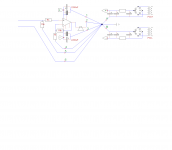
If that is what Pj has assembled, then I don't agree with much of what has been implemented.
It basically breaks the "rule" to keep Loop Areas of each circuit as small as possible.
eg.
look at the input circuit.
Signal Hot comes in from Input Socket, passes the Rin tapping, through Rb to +In. A fairly simple route.
Signal Return comes in from the Input Socket, goes to MAG, comes back from MAG to go through Rin into the Hot route.
That is a long route that is not necessary and includes lots of loop area and worse because of the LONG wire lengths must have high inductance.
That inductance will have a different impedance from the short Hot route. Is that more interference?
Local decoupling has long routes.
NFB tapping has a long route.
The issue is not "swamping" but simply keeping charging current pulses in their own circuit loop. Always design grounding by thinking about where the currents go - don't blindly follow a recipe, unless that is all you can do.bentsnake said:The idea here is that very large current pulses flow in the power supply, and very dirty hash is injected into ground by the bypass/decoupling capacitors. The plan is to have these distortions swamped by the transformer and smoothing capacitors, so they don't distort the much smaller input signal. By the way, "swamped" really is an engineering term.
Don't have two stars: one for signal, one for PSU. Instead, use a ground bus in the PSU with the transformer CT at the dirty end, the reservoir ground in the middle, and any smoother or PSU-based decoupling caps at the clean end - which then connects to the signal ground (which may include the speaker return). Make sure any NFB is related to the voltage across the speaker, not some other voltage.
PS I have never found a reason to use extra flux. Just use good quality electronic solder, an appropriate iron for the job, and learn how to solder. Not all solder sold for electronics is good quality! If it looks cheap, avoid it.
Last edited:
.
<< Don't have two stars >>
You contradict Douglas Self in "Audio Power Amplifier Design Handbook," also in "Self on Audio." Also the engineering department of Texas International in the reference given. Among others.
Of course if you know something they don't, then power to you. But it would be nice if you either showed your math, or gave a reference. Speaking only for myself, I can't say that your bald statement of "don't" is convincing.
Musing: In the "ground bus" you speak of the poor audio signal first has noise injected from the decoupling/bypass capacitors, then is subjected to the huge DC pulses occurring in the reservoir/smoothing capacitors, then at last finds sweet oblivion in the swamping effect of the transformer coils. The band will now play "Didn't He Ramble."
<< The issue is not "swamping" but simply keeping charging current pulses in their own circuit loop. >>
The issue is both. At some point the various loops must join, obviously. So then then where does the noise go?
<< ...learn how to solder. >>
Well yes, that would be the point exactly. The idea is to set somebody up so they can learn instead of fail.
.
When people tell me I have contradicted someone else I usually leave others to judge. Vicarious disagreement is rarely useful in technical discussions.bentsnake said:You contradict Douglas Self in "Audio Power Amplifier Design Handbook," also in "Self on Audio." Also the engineering department of Texas International in the reference given. Among others.
The issue, as I said, is keeping charging pulses away from the signal. A PSU bus does this; a PSU star does not (unless very carefully executed - such as ensuring that tags go on in the right order, in which case you then have a 'vertical bus'!).
The "poor audio signal" is kept well away from the PSU ground bus. I have no idea what you mean by "the swamping effect of the transformer coils".Musing: In the "ground bus" you speak of the poor audio signal first has noise injected from the decoupling/bypass capacitors, then is subjected to the huge DC pulses occurring in the reservoir/smoothing capacitors, then at last finds sweet oblivion in the swamping effect of the transformer coils.
Eh? What noise? Signal currents stay in their loops. PSU currents stay in their loops.The issue is both. At some point the various loops must join, obviously. So then then where does the noise go?
As
Last edited:
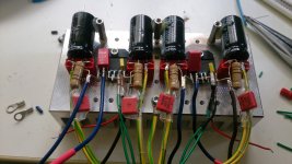
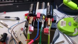
I think this is close to what Pjotter has build. I left out the RC to GND.
Yup, this is pretty much what i've done.
If that is what Pj has assembled, then I don't agree with much of what has been implemented.
It basically breaks the "rule" to keep Loop Areas of each circuit as small as possible.
eg.
look at the input circuit.
Signal Hot comes in from Input Socket, passes the Rin tapping, through Rb to +In. A fairly simple route.
Signal Return comes in from the Input Socket, goes to MAG, comes back from MAG to go through Rin into the Hot route.
That is a long route that is not necessary and includes lots of loop area and worse because of the LONG wire lengths must have high inductance.
That inductance will have a different impedance from the short Hot route. Is that more interference?
Local decoupling has long routes.
NFB tapping has a long route.
Great, thanks for the input. It really helps me making something that i couldn't have done all by myself.
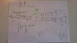
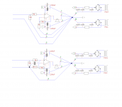
I've included a schematic I've drawn, it's basically how everything is connected right now.
However i didn't included the "pre amp" stage in this schematic.
Perhaps i should have done that, if necessary i can do this.
Attachments
.
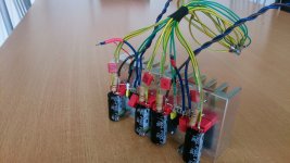
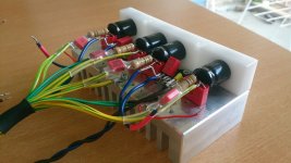
Pjotter, whoa, nice looking work! Not to mention interesting use of hardware.
Sorry, but I have to say a word about hot glue. It works at around 300 degrees F, which is way hotter than the design specs of most components.
Meanwhile, I might as well finish the thought from post #21. The first circuit posted below is essentially the same as in post #21, re-posted just for convenience. The second circuit is a detail of the power supply connections.
The second circuit is simpler that it might seem just at a glance. Internal to the power supply there is:
1. A jumper from the ground side of the bypass capacitors to the transformer center tap, and:
2. A jumper from the ground side of the smoothing capacitors, also to the transformer center tap.
Otherwise things are not much different. The "signal ground" is the same zero-volt ground you expect to see on a power supply.
All of which commits pretty serious violence upon the rule of "One circuit, one ground, always and only." I'd actually much rather refer to a signal common, and a chassis common, therefore calling the Main Ground simply ground. But it appears popular usage decides otherwise, and I know what to do when I'm outnumbered (run).
As before, this is my understanding of the references cited (many times checked). If I've misinterpreted or misunderstood anybody I'd be very happy to be corrected by them.
.
Attachments
Last edited:
")
No charge; my advice is free. There are a number of satisfied customers on here, though: people who had hum/buzz problems with one or two stars, but got beautiful silence when doing it the way I suggest.bentsnake said:No, sorry, but you're still selling your ground bus, and I already told you I'm not buying.
It isn't my ground bus; I saw others advocating it, thought about it, and decided that they were right - circuit theory rules!
What rubbish. If the joints are clean the flux in the solder is more than adequate. Extra flux only adds corrosion problems later in life.
Copper is absolutely fine but you do need heavy gauge wire especially for the 0V (GND) connections, and the power rails. The output wiring should also be substantial.
There should be no problem with new parts, when soldering with the normal types of electronic solder with integral flux.
However, old oxidized parts will be a problem sometimes. Those should be scraped off to a fresh surface prior to soldering,
rather than relying on flux alone.
Last edited:
The Speaker current comes from the PSU, it has to return to the PSU.Trace out the ROUTE that the current takes in flowing from the PSU through the amplifier to the Speaker. It is a long route, think carefully about each part and don't miss any part out. It's a little bit easier if you consider only the +ve half of the AC waveform and follow that through the +ve half of the output stage. and DON'T miss out the local decoupling caps. They pass the fastest changing currents and create the highest interference fields. Mark refers to "bypass capacitors", I think he meant local HF & MF decoupling capacitors.The RETURN ROUTE must exactly follow that FLOW ROUTE.And twist wherever possible.
You have all that exactly right, i's just difficult to put into words clearly. The same ideas apply to pcb layouts.
Last edited:
- Status
- This old topic is closed. If you want to reopen this topic, contact a moderator using the "Report Post" button.
- Home
- Amplifiers
- Chip Amps
- Internal wiring for ChipAmp, Silver? Copper? Gold plated? Thickness?