Innovation in the world of semiconductors, computing, fabrication, machinery, industrial processes, natural resource extraction:
I deleted the text I wrote here discussing a model for the structure of new initiative propagation in the industry. The purpose of the text was to explain that imitation follows 3 thermodynamic laws.
The text seemed to contain some statements in conflict with moral conventions at some parts of the world. I deleted it. However, I can say that: Individuals who never accept their vulnerabilities to be scanned and listed by a friendly auditor may at some point face the situation of having their vulnerabilities scanned and listed by a non-friendly auditor.
Last edited:
OK, lets expose today's example:
The new DDPAK from Infineon: Power Systems Design (PSD) Information to Power Your Designs
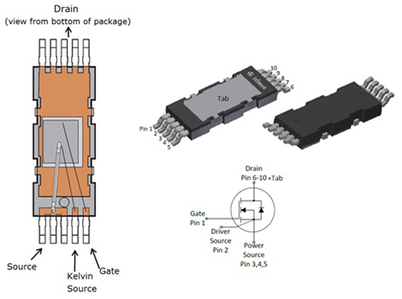
- Claiming half the inductance of TO-220 for a package with more loop length. What inductance were they considering?
- Claiming higher thermal conductivity than TO-220 for a package with half of heat transfer area and less thermal mass.
- Claiming the suppression of one manufacturing step that is needed anyways (bottom side selective soldering for thru-hole parts) in attempt to compete with other countries' economy, whose tricks are cheap labor, finding conditions for workers to be happy with less expense, and more manufacturing steps to prevent unemployment or excessive expansion of non-technically-competitive sectors (which happens to be the same).
- Claiming reduction of distance from PCB to heatsink is good for power supplies, while it prevents mounting (always taller) diode bridges to heatsink, it prevents using (always taller) Reinforced Insulation optocouplers on bottom side of PCB, it mandates the usage of a custom cut insulation sheet between PCB and heatsink for off-line applications.
The new DDPAK from Infineon: Power Systems Design (PSD) Information to Power Your Designs
- Claiming half the inductance of TO-220 for a package with more loop length. What inductance were they considering?
- Claiming higher thermal conductivity than TO-220 for a package with half of heat transfer area and less thermal mass.
- Claiming the suppression of one manufacturing step that is needed anyways (bottom side selective soldering for thru-hole parts) in attempt to compete with other countries' economy, whose tricks are cheap labor, finding conditions for workers to be happy with less expense, and more manufacturing steps to prevent unemployment or excessive expansion of non-technically-competitive sectors (which happens to be the same).
- Claiming reduction of distance from PCB to heatsink is good for power supplies, while it prevents mounting (always taller) diode bridges to heatsink, it prevents using (always taller) Reinforced Insulation optocouplers on bottom side of PCB, it mandates the usage of a custom cut insulation sheet between PCB and heatsink for off-line applications.
Last edited:
Dear Madam (considering your first posting),
As you live close to the sea, give the sea a glance before you rank the qualities of superiors in your region:
* Politically conform
* Financially focussed
* Competitive
* Technically innovative
* Motivating
* Static
* Control freak
* Inapproachable
You, Madam, belong to a class loosing ground because progress is seen as a challenge to control.
Last edited:
This is a good example of the phenomena being exposed:
A speech about competitiveness which relies in discarding measurable physical magnitudes. Individual is relying in a relationship which relies in discarding competitiveness in physics. Members of the relationship have contradictory experience about physics.
The initiative is neither coming from human testosterone logic, nor targeted to human testosterone logic. It is seek for female type acceptation (irrational attraction, estrogen), powered by animal testosterone (growl).
Last edited:
OK, lets expose today's example:
The new DDPAK from Infineon: Power Systems Design (PSD) Information to Power Your Designs <snip>
I've seen this package used in micro inverters.
I think eva is saying that Infineon are needlessly reinventing the wheel and its causing quite a few issues. Reinventing the wheel is like the oscillation in a circuit they must reinvent things to remain innovative, keep people in jobs, create pollution and waste. etc.
I couldn't agree more with that viewpoint if my viewpoint is correct.
I couldn't agree more with that viewpoint if my viewpoint is correct.
The new DDPAK from Infineon:......Infineon are needlessly reinventing the wheel
Unique semiconductor packaging schemes are easy patents to get, so sometimes that's the only reason they exist.........
Note, I coauthored two such patents for stuffing multiple die in a single package to share a common heat sink since only one die was turned on at a time. One of these was granted US patent #7,259,446. The other was filed and approved, but Motorola deemed it no longer useful and therefore it was abandoned before being issued.
Neither was actually used in a product since we developed the broadband RF Power Amplifier during the time between these patent applications and patent grant, therefore the multi die package was not needed.
A range of new SMD packages, intended for not using the PCB as the heatsink, are required. I have often run into applications that benefit from these packages.
But that "DDPAK" is not that well executed. Inductance is not better than TO-220. That project has not been checked by a true high speed switching designer. Half of drain and source connections should be at the same side of the package.
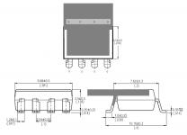
And to complete the line, for high power and pulsed applications, someone should make a SMD-friendly version of classic TO-220, like a SMD DIP-8 with thick power pad (providing thermal inertia) larger than package outline. Sketch is attached.
But that "DDPAK" is not that well executed. Inductance is not better than TO-220. That project has not been checked by a true high speed switching designer. Half of drain and source connections should be at the same side of the package.
And to complete the line, for high power and pulsed applications, someone should make a SMD-friendly version of classic TO-220, like a SMD DIP-8 with thick power pad (providing thermal inertia) larger than package outline. Sketch is attached.
Attachments
Often, as with the SMD packages I designed, a specific application is known in advance and a unique package is made for it. Designing a new package comes down to the usual two main criteria, need for something new, and cost savings X expected sales volume. The sales volume thing is the MAIN driver in today's market, and the reason why many low volume parts are dying off today. If a new semiconductor component doesn't find a million part per year socket within a year of so, it will go away.
Ours were low source inductance packages for 100 MHz to 1GHz radio transmitters. The LDMOS die had the source terminal as the substrate which was bonded directly to the lid / heat sink. Then the remainder of the package was built upside down. Wirebonds were used for the gate and drain terminals which were routed to SMD pads for the PC board. Our needs were unique, the sales volumes were very low by todays standards (50K/yr) but the profit per unit was very high, so we HAD to design our own SMD packaging. Nobody in the business would do it.
Solderable by the usual automated SMD processes, but some pick and place machines may not like the offset design.
Ours were low source inductance packages for 100 MHz to 1GHz radio transmitters. The LDMOS die had the source terminal as the substrate which was bonded directly to the lid / heat sink. Then the remainder of the package was built upside down. Wirebonds were used for the gate and drain terminals which were routed to SMD pads for the PC board. Our needs were unique, the sales volumes were very low by todays standards (50K/yr) but the profit per unit was very high, so we HAD to design our own SMD packaging. Nobody in the business would do it.
Interesting, but impossible to solder.
Solderable by the usual automated SMD processes, but some pick and place machines may not like the offset design.
Solderable by the usual automated SMD processes, but some pick and place machines may not like the offset design.
I think the overhang would shield the legs from being heated sufficiently by the usual automated process.
But the industry seems to want a package that's cheap to build and cheap to assemble at the next higher level. Putting high power RF in a QFN lead frame, for instance. The thermals are a b**** with a cheA-p pcb. Better performance can be had with a coined board or whatever, but the price of your product just went stupid and put you out of the market. Plenty of high performance SMD packages exist - many of them custom or semi custom. And they usually require specially-machined heat sink assemblies that are labor intensive to assemble with the rest of the circuitry. Expensive and very application specific. You just won't find the latest generation of class D power transistors (or igbts for the supply ) in them - and if you did they would be $100 apiece with a 5k piece minimum order and 26 week lead time.
I think the overhang would shield the legs from being heated sufficiently by the usual automated process.
We had our own SMD assembly lab that would do prototype runs of up to 1000 boards. I ran some boards that had overhanging heat sink experiments without issue, but we were NOT using lead free solder. The lab would do either kind of solder, but we used lead for prototypes because we had to work on these boards and were not shipping them anywhere.
The trick to some of these unique assemblies is to preheat the board from both sides to near melting before the final heat soak from the top. These kinds of parts and all heavy parts like SMPS inductors must be all on the same side, which gets built last.
cheA-p pcb. Better performance can be had with a coined board or whatever
We had our own in house board lab too. I could get things like a multi layer board with 2 layers of Rogers and the rest FR4. We tried embedded heat spreaders and other tricks, but our hand held two way radio products must be able to transmit continuously for up to 5 minutes at 5 watts of power output with about 60% efficiency. We had to get the heat out of the board.
The area under the tab will also heat to soldering peak temperature. If timing is proper everything heats to peak temperature. Since elastomer thermoconductive pads are required anyway to compensate uneven offset and bending of PCB, loss of flatness in the tab due to melting of solder coating is not a problem.
Industry wants packages that can suit a wide range of applications. A SMD TO-220 is preferable in SMD boards. A SMD TO-220 would quickly become a replacement for TO-220 in SMD boards, as for power supplies and amplifiers. Many attempts were made to create this replacement but all seemed to be more optimized for some application.
There is also the option of creating a machine for machining TO-220 into SMD ready to be loaded into pick&place machine, and using another machine to apply dots of glue to the boards at center of TO-220 locations before entering pick&place machine.
I agree that power SMD devices transferring heat to the board soon runs short, or ages fast. Heat transfer to the board was an idea for signal boards, with stable slow-changing working temperature. The SMD power transistor/diode packages imitating TO-220, upside down, were originally intended for strong-pulsed low duty cycle applications.
- Status
- This old topic is closed. If you want to reopen this topic, contact a moderator using the "Report Post" button.
- Home
- Amplifiers
- Class D
- Innovation in the world of semiconductors, computing, fabrication, machinery...