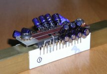
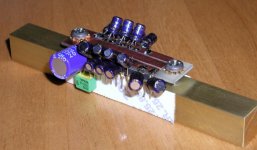
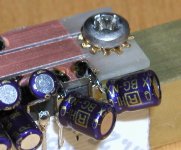
Initially I was considering PCB, but somehow didn't like the restrictions dictated by 2 dimentional plane. So last evening I took a piece of brass and played with it a bit. I mounted the chip on top of 1/2 square rod and attached to it on top a piece of PCB forming ground plane. The rest is pretty self explanatory. I wonder myself if this is a good move or not?")
Any comments on 560p Wima? I didn't know if this a good choice, but that's what seemed to fit there.
Any comments on 560p Wima? I didn't know if this a good choice, but that's what seemed to fit there.
Attachments
I was thinking about splitting grounds, but checked the PCB board on my Marantz CD 94 and both grounds were connected at the chip (same ground plane). Doing it this way definitely simplifies things, but I'm not sure how this affects sound. If they are separated at the chip, were should they meet then?
Pedja said:Hi Peter,
Yes, it is OK I'd say (excellent actually), but try to divide digital and analog grounds before you joint them. Decoupling caps (pins 26 and 28) belong to the digital, those 14 caps to the analog part.
Pedja
So 5v supplies are digital and -15 is analog? I could use a center ground strip to route grounds from pins 26 and 28 to the common point on the other side.
Somewhere below/above the chip. Just make sure that the analog and digital ground paths are not messed, i.e. provide that the digital part doesn't polute an analog part.Peter Daniel said:If they are separated at the chip, were should they meet then?
Yes.Peter Daniel said:So 5v supplies are digital and -15 is analog?
Pedja
Yes, it seems like you have three nice ground buses.Peter Daniel said:So 5v supplies are digital and -15 is analog? I could use a center ground strip to route grounds from pins 26 and 28 to the common point on the other side.
Nice work, Peter!
I've found that these DACs benefit enormously from good PSU decoupling and screening and it isn't possible to optimise this using a PCB alone.
As regards connecting analogue and digital grounds: ignore the method used by Marantz, on my CD80 they're daisy-chained together by a thin track . They should meet at a low impedance point like a big decoupling capacitor.
I've found that these DACs benefit enormously from good PSU decoupling and screening and it isn't possible to optimise this using a PCB alone.
As regards connecting analogue and digital grounds: ignore the method used by Marantz, on my CD80 they're daisy-chained together by a thin track
. They should meet at a low impedance point like a big decoupling capacitor.Thanks.Peter Daniel said:Pedja,
I just checked your site and the info is good as usually (on TDA1541 Dac)
No doubt, it benefits. I screened the chips by the copper sheets later but still have to upload newer pics. And yes, the way the Peter is doing this might be better than usage of PCB, regardless of how careful it is designed. Though it is certainly not the easier way.Richard C said:I've found that these DACs benefit enormously from good PSU decoupling and screening and it isn't possible to optimise this using a PCB alone.
Two pages of extremely useful text on the topic:As regards connecting analogue and digital grounds: ignore the method used by Marantz, on my CD80 they're daisy-chained together by a thin track
http://www.sigcon.com/Pubs/edn/adcgrounding.htm
http://www.sigcon.com/Pubs/edn/multipleadc.htm
Pedja
Pedja said:Also, though it doesn't hurt, that jumper between pins 2 and 4 shouldn't be necessary.
Pedja
I see it is both on Marantz schematic and Thorsten DAC. What is the reason for it?
Pretty as always. Have you also consider to mount the receiver chip in the same manner, but face it inverted and mount it underneath the DAC chip. This way, the 3 I2S pins (FSYNC, SCK, SDATA) will be P2P also. This will solve your ground plane problem too, by sandwiching a ground plane (say digital ground under the chips) between the two chips. Analogue ground will be on the top of both chips.
Peter,
You are crazy
I would suggest not using any cap between pin 16 & 17, but instead implement the DEM reclocking circuit.
You'll be suprised how much it does.
Thread about DEM is somewhere in the archives.
BTW TDA1543 board is finished, just need to install it in a cd player. Probably start a thread tonight.
TDA 1541 circuit is mostly based on this http://www.fortunecity.com/rivendell/xentar/1179/projects/adagio/Adagio.html
The reast will be based on this http://www.diyaudio.com/forums/showthread.php?s=&threadid=23044
because it sounds good I won't be using input receiver, I2S from transport goes directly to DAC (through reclocking circuit)
The reast will be based on this http://www.diyaudio.com/forums/showthread.php?s=&threadid=23044
because it sounds good
I won't be using input receiver, I2S from transport goes directly to DAC (through reclocking circuit)- Status
- This old topic is closed. If you want to reopen this topic, contact a moderator using the "Report Post" button.
- Home
- Source & Line
- Digital Source
- I must be crazy to build my DAC this way