Hi, Ionutgaga,
Ah, yes the 0.5ohm resistor. Thanks.
Why is that when I read Kanwar's post, my thinking don't go to that resistor, but I'm thinking about friends of strain gage stuff (lab measurement equipment).
If one resistor is on +rail, the other one on -rail, the common for osciloscope goes to gnd, scope goes to AC mode?
Ah, yes
the 0.5ohm resistor. Thanks.Why is that when I read Kanwar's post, my thinking don't go to that resistor, but I'm thinking about friends of strain gage stuff (lab measurement equipment).
If one resistor is on +rail, the other one on -rail, the common for osciloscope goes to gnd, scope goes to AC mode?
Probes are not strictly required. You will find that the derivative of drain current is superimposed on top of the Vgs waveform when measuring directly at transistor leads. The value of commutation di/dt is quite easy to find out and tune by just looking at Vgs. The magnitude of the current spikes may be guessed too by integrating di/dt during the time it lasts.
Hi, I have a problem with recovery diode in half bridge class D. In my design, I inserted a RCD network before IR2110 driver. This network gives around 200ns delay to my turn off / turn on of complementary mosfet's. My mosfet's are IRF640n, and in my circuit I get near 3A of reverse current in reverse diodes when the modulation index is near 80%. I also added soft recovery diodes in parallel to gate resistors in order to control dv/dt in body diodes. My project works perfectly with 40V rails, the dead time is not optimized for THD, I know that I can optimize it by current signal inspection on the mosfets.
My question is about recovery time, and delay time added in order to prevent shoot through. I can not view how this death time can prevent excesive reverse current in freewheeling diodes. I know that when a totem pole is driving an output signal with high modulation index, the inductor output current never changes his sign, and the mosfet that is carrying only the conmutation current, never changes the voltage of the bridge output because the freewheeling diode is forward biased before the mosfet goes to off state (¿the gate turn off of this mosfet changes nothing?). How can the delay time prevent shoot through if the diode can't block reverse voltage until reverse recovery current provides Qrr? The reverse recovery current, isn't supplied through the complementary mosfet when turns ON?
I'm very confused with this, and I can not understand this recovery current event. How can the diode go to off if in the duration of this dead time if this Qrr charge is not supplied by any device?
I suposse this is an evident thing, please can help me someone?
Thank you very much and regards.
PD:Sorry for my english.
Juan Carlos.
Attachments
Just to confirm what Eva said earlier.
The gapped 3F3 ferrite toroids from Ferroxcube are ideal for winding class-D output inductors. It's what the cores were intended for after all (see the Ferroxcube app-note on this subject). It's dust-iron toroids that are very lossy as output filter inductors.
The gapped 3F3 ferrite toroids from Ferroxcube are ideal for winding class-D output inductors. It's what the cores were intended for after all (see the Ferroxcube app-note on this subject). It's dust-iron toroids that are very lossy as output filter inductors.
Anyone can explain me the effect of the dead time in te reverse recovery characteritic? Please, I'm very confused and I cannot understand the reverse recovery. The current through the wheeling diode, reverses during dead time???(this is not possible, I'm missing somethig).I know that If I turn down complementary mosfet turn on, I limit the dIrec/dt, and the I limit IRR, Qrr and trr, but,
what happens if I add this time delay? how affects recovery in the diode?
Juanqui.
what happens if I add this time delay? how affects recovery in the diode?
Juanqui.
Then, the delay time, only is designed to account for the time delay to off state "td(off)" and to the time fall "tf" to the off state of the mosfet in order to avoid cross conduction. And with the gate resistor-diode network, we can adjust Qrr losses and dv/dt capability. Optimal adjust for efficiency will be do by turn on mosfet losses and Qrr inverse diode losses adjust (without forgetting dv/dt).
In my design, I go near 200ns delay time between IRF640N at a switching speed Fsw 420KHz at idle. I can not reduce this time too much. In the IRF datasheet is specified max toff= 46ns, I suppose this time would grow up with the pcb inductances limiting Cg discharging (Right?), so, the conclussion is:
"I need to learn more about pcb for SMPS design"
Thank you very much to Ouroboros for opening my eyes.
Juanqui.
Hi. I tried to minimise dead time in my design, but I can't reduce it too much. I have near 200ns. How is possible, if the maximum time specified in the IRF640N is Toff=46ns(Tdelayoff+Tfall for VDD= 100V, ID= 11A VGS= 10V, RGS= 2.5Ω)?. I have Vdd=80V, Id= 10A, Vgs=15V y RGS= 33Ω with paralell ultrafast diode.
I tried in simulation, and in my PCB prototype. I supose parasitics is not the problem. I designed the board to minimise high current loops in driver output section and in the output stage. How can I minimise this dead time?
Thank you very much and regards.
Juan Carlos.
I tried in simulation, and in my PCB prototype. I supose parasitics is not the problem. I designed the board to minimise high current loops in driver output section and in the output stage. How can I minimise this dead time?
Thank you very much and regards.
Juan Carlos.
Attachments
I tried to minimise dead time in my design, but I can't reduce it too much
Because...?
Lower C2, C4, Rg-> smaller DT. What do you really want to achieve?
BTW: IRF640N is not the best MOSFET for ClassD audio. Its diode is too slow.
I tried to decrease with R25,R24,C4,C2. How affects Rg dead time? I have diodes for fast gate discharging.
If I reduce this 200ns dead time, i get destructive current spikes with high modulation index. If the Toff is near 56ns máx, Can't I reach this time for the delay time?
I don't want replace the IRF640N, my intention is understand the half bridge operation.
Thanks for your attention
If I reduce this 200ns dead time, i get destructive current spikes with high modulation index. If the Toff is near 56ns máx, Can't I reach this time for the delay time?
I don't want replace the IRF640N, my intention is understand the half bridge operation.
Thanks for your attention
Use oscilloscope to find out which edges are overlapping and which ones are not. You may find useful to synchronize the display with the outputs of the comparator in order to find out what happens to the edges of the signal on its way to the gates. Be aware that probe capacitance will alter pulse timing somewhat.
Note that propagation times may be signal dependent (usually when the circuit is not good, a too small bootstrap capacitor is employed, etc..) leading to cross-conduction (or the lack of) only in some circumstances.
Note that propagation times may be signal dependent (usually when the circuit is not good, a too small bootstrap capacitor is employed, etc..) leading to cross-conduction (or the lack of) only in some circumstances.
How affects Rg dead time?
It makes tdon longer.
If I reduce this 200ns dead time,
Are you sure this 200ns exists at high modulation index too?
i get destructive current spikes with high modulation index.
Have you measured these current spikes, or just deduced? How high modulation index? How much output current?
IR2110 (and maybe all other IR high side driver) have a known fault: with very narrow positive impulses on Hin, it can be latched, Hout stucked in high state. Maybe you've experienced this.
Otherwise I agree with Eva, you should measure everything with scope, with low capacitance probe.
For low currents the circuit will work in resonant mode with no current spikes, except in case something is really wrong. Body diodes will not conduct. Inductor current will change direction during each half cycle.
When inductor current becomes continuous but moderate, the voltage drop on Rds-on will usually be low enough to prevent the body diodes from conducting, except during dead time when both MOSFET are off. In this state, longer dead times result in more charge stored in body diodes and taller recovery spikes.
At high current levels, when Rds-on is not low enough to prevent body diodes to conduct, there is enough time for the full Qrr to be stored resulting in the strongest recovery spikes. Many MOSFET models and PCB layouts will not be up to the job. The gate drivers may become stressed too, and sometimes they may require protective schottkys from the outputs to ground (near chip leads) to avoid failure or latching due to excessive reverse bias. Voltage spikes will result from abrupt changes in the amount of current flowing through MOSFET source lead inductance and will become coupled to the gate. They may be as tall as +/-5V. RC snubbers may be useful in controlling the spikes too, both from D to S and from G to S.
BTW: IRF640N is a very bad choice. You will have real trouble making it reliable at high currents when the body diodes become fully turned on.
Concerning the IR2110 latching behaviour on short pulses, is there any application note on the subject?
Thank You
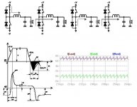
Finally, I just understand mosfets in half bridge. Thank you so much to Pafi & Eva. I finally can reduce the dead time to 50ns (substituting IR2110 in the circuit by a PWM signal source in the mosfets gates) . The problem was in IR2110. I get terrible shoot trough current spikes when the low side mosfet go on (near 70ns dead time 50% modulation). This is caused by a reduced speed in the high side gate discharge (tested in simulation), is this possible? the gate signals are overlaped only when the Low side go ON and the High Side OFF. Should I adjust dead times for low side and high side separately?
I can not change anything in circuit. I build the circuit for a final career project. I can not replace components without damage, and I have no time to experiment more with the circuit. But in the future, I would like to add improves to the circuit (too much improves).
Thank you guys so much.
Juanqui.
Attachments
Are you talking about simulation or about the real circuit? Simulation of that kind of circuits is completely useless, no matter what they have teached you. Don't waste your time, too many details about the real circuit are not being included in the simulation.
In my current project I use two IR2110 in a full bridge arrangement (200V) to produce up to 3KW on 4 ohms. There is no dead time. It seems to be working reliably. In this IC the timing of the high and low sides is very well matched, even when the chip gets hot. I don't use IR2010 because timing matching is not that good. The only source of mismatching that I have found is supply voltage, which should be in the 15V range. I even had to correct the 7ns delay due to the 74HC04 inverter used to obtain the high side signal from the low side one (it manifests as a 14ns difference in dead times).
In my current project I use two IR2110 in a full bridge arrangement (200V) to produce up to 3KW on 4 ohms. There is no dead time. It seems to be working reliably. In this IC the timing of the high and low sides is very well matched, even when the chip gets hot. I don't use IR2010 because timing matching is not that good. The only source of mismatching that I have found is supply voltage, which should be in the 15V range. I even had to correct the 7ns delay due to the 74HC04 inverter used to obtain the high side signal from the low side one (it manifests as a 14ns difference in dead times).
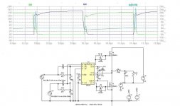
This is simulation. I will try in the circuit (I really expend a lot of money in mosfets and mosfets drivers for this design because is my first time with power electronics, and for the moment, I don't feel really comfortable with real circuit measurement and components adjustment), but I suppose that I will need to insert RC snubbers in order to minimisse resonances in switching waveform. In my circuit, I insert shunt resistors for current measurement. Before the insertion of this resistors, I get clean switching waveform, but this resistors degraded switching behavior.
In the future, I would like to mount full bridge IRF540Z, IRS20955(overcurrent protection built in) and LT1016 (this is no new configuration in this forum, but I need to experiment with switching mosfets because I'm novice in this area).
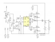
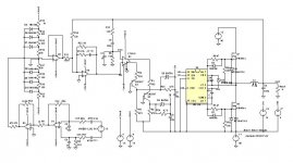
In the attached file, my complet circuit without current and DC protection.
Thanks .
Juanqui.
The more I learn more I feel ignorant.
In the future, I would like to mount full bridge IRF540Z, IRS20955(overcurrent protection built in) and LT1016 (this is no new configuration in this forum, but I need to experiment with switching mosfets because I'm novice in this area).
In the attached file, my complet circuit without current and DC protection.
Thanks .
Juanqui.
The more I learn more I feel ignorant.
Attachments
Eva, referrent to Mosfets power losses, can I use this formula from AN-1070 IRF "Class D Audio Amplifier Performance Relationship
to MOSFET Parameters"?
PSWITCHING = [0.5 * ID * Vbus * (tr + tf) * fsw] + [0.5 * Coss * Vbus
2 * fsw] + [K * 0.5 * Qrr * Vbus * fsw]
What is this K factor needed to calculate diode Qrr losses?
Thanks.
to MOSFET Parameters"?
PSWITCHING = [0.5 * ID * Vbus * (tr + tf) * fsw] + [0.5 * Coss * Vbus
2 * fsw] + [K * 0.5 * Qrr * Vbus * fsw]
What is this K factor needed to calculate diode Qrr losses?
Thanks.
- Status
- This old topic is closed. If you want to reopen this topic, contact a moderator using the "Report Post" button.
- Home
- Amplifiers
- Class D
- How to minimise crossconduction