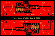
Please take into account this is my first real stab at a board. I made it with expresspcb, but all traces will be on the bottom, I put them on the top here for easier viewing. If it looks good, I will try to make my some by myself.
The 2 will be seperated and mounted individually.
The 2 will be seperated and mounted individually.
Attachments
Peter Daniel said:I'm not that familiar with pin out on OPA541, but it seems like feedback loop path is unneccessarily long.
I've noticed that too.
")
Trigon.
looks great for a first board, congrats for making the effort.
so yea if u can just fix up that overlly long feedback , which i assume is going from the bottom of the 22k round the back to the output then to 2nd pn from left?? , then it should be closer to the mark, unfortunatly thats one of the very crucial factors of a good gainclone.
would u consider P2Ping the feedback resistor.. like in my mock up here.
(the 1 running horizontal along the top)
i know its not as neat as a pcb but its the shortest path possible isnt it
so yea if u can just fix up that overlly long feedback , which i assume is going from the bottom of the 22k round the back to the output then to 2nd pn from left?? , then it should be closer to the mark, unfortunatly thats one of the very crucial factors of a good gainclone.
would u consider P2Ping the feedback resistor.. like in my mock up here.
(the 1 running horizontal along the top)
An externally hosted image should be here but it was not working when we last tested it.
i know its not as neat as a pcb but its the shortest path possible isnt it
mAJORD said:i know its not as neat as a pcb but its the shortest path possible isnt it
Beware of those naked wires!!!
Use some teflon spaguetti to protect from shortcircuits and oxidation.
The former is quite likely to happen in the assembly, and Murphy's law is dominant in p2p.
Carlos
FYI: When you print Express PCB stuff, it leaves a dark board area to make it very difficult to create home-brew PCB's. They want you to order them... 
Here is the solution: before you print your final artwork, double click all the board corners and put in the coordinates "0,0" for all spots. The board outline will disappear and you will be able to print the layout and do any sort of transfer to PCB. It does still leave a .1" grid, but the dark fill color of the normal style printing disappears.
-Matt
One more thing...add some copper around all your holes, becuase the pads in ExpressPCB were done for thru-holes, they are very difficult for most of us to drill accurately, and even if drilled properly, the solder joint won't hold well without that plated-thru hole. Just make the resistor pads there have some more "beef" so the thing will hold together like it should.
-Matt
-Matt
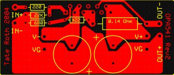
Thanks everyone, I had a lot of fun designing the board and I have already taken some suggestions, making the feedback path shorter, and created my Version 2 below. How does this one look?
I found an easy way to use the layout from express pcb. I just use the view option to remove the grid, hide the overlay, and make the background white. Then I blow it up and screenshot it into photoshop. My next post will have the layout for my first design done that way. I may end up making both to see how different they are.
Thanks for all the help.
Peanut
Attachments

zagisrule! said:You need to beef up that output trace or you will be smoking some copper!
Fun!!! Burning copper!!
![opa541 v1[1].0.jpg](/community/data/attachments/21/21774-7c2985be43280ad4bf191e52061ae78b.jpg)
I have a newer version 1.1 that I will post tonight that has revised resistor locations and shorter traces. The really thin trace on my boards connects to the current sense pin and needs to connect after the big resistor. Pins 5 & 7 are the drive pins. I beefed up the trace before and after the big resistor to 0.15" traces.
Once you can use the copper rectangle tol, you might go back and enlarge the pads a bit on the lone components so that the solder has enough to "bite"
Also, I would use traces at least .025" - .04" where they will fit....015" is still quite small.
I guess it is an aquired skill, I have done tons and am still learning more each time. The first few are the hardest, but you need to set a foundation of how to do things so the next ones will come out like they should.
-Matt
- Status
- This old topic is closed. If you want to reopen this topic, contact a moderator using the "Report Post" button.
- Home
- Amplifiers
- Chip Amps
- How does my board look?