My 1981 microwave oven has a conventional transformer supply, including the low-volt, and was damaged by a lightning strike.
One place, linear-supply modems and answering machines were dying two every summer. (This was an extreme case: underground power but overhead phone line, and a telephone protector block from the 1910s.)
"Whole House" lightning/surge protectors exist and some are good. "Surge" outlet strips are good secondary protection. It is also good to know that your power entrance (line from the company) has all locally required "earthing"; I studied Code and added a jumper at my (private) pole and also 3rd 4th 5th dirt-rods for luck. (Dirt here is very thin and one rod is just wishful thinking.)
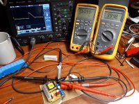
So I bought one of these Chinese PSU
DC-DC Boost Converter 8~32V to 45~390V High Voltage Charging Booster Module 40W Sale - Banggood Mobile
I will echo others comments, it doesn't seem too bad, considering the price. I have been quite busy testing it the last week or so.
The voltage regulation seemed off at first, so I changed the voltage adjustment trimmer.
It worked a whole lot better after that...
P.S. Using a 10k rather than the installed 50k, limited the output range to 143-390
What I have found is that it is ZVS type (I have the single rail version, although there is a dual rail version also).
Due to this, and despite the constant switching frequency which according to my scope is near 48kHz, rather than the advertised 75kHz, the burst switching/pulse dropping action results in voltage ripple which modulates the carrier ripple (which is actually pretty low in level at about 80mV pk-pk).
What this means is that dependant on the desired output voltage, current draw, the ripple is variable.
I have found that I can achieve anywhere between the baseline 80mV HF hash, and up to 15 Volts modulated at around 10Hz. The latter case at higher voltages.
I don't fully understand the relationships here, but testing with various resistors to give a constant load, I find a few sweet spots in voltage, which do move about, when the current drawn is changed.
These sweet spots have low ripple in terms of AC percentage, but how they react to an active load?.....that will come in time I suppose.
I'm planning to run a tube line stage, preamp, or head amp so I will probably try and set up the PSU so I have minimal ripple with the span of current draw I expect in use, and hope that means I avoid ripple above say...1% of DC output.
Once I have finished tabulating my results, I'll post the graphs.
Last edited:
Some data
Some data taken in testing this £3 SMPS PSU from ebay (attached PDF)
Cheaply made but seems like not too shabby a supply (as long as you check joints, connections and don't expect miracles) - After 30 mins at rated 40W dissipation the transformer is the hottest part, other than the loading resistor!!!
Personally I'd limit it below 30W, or fan cool as soon as the unit is boxed up.
I have taken ripple factor measurements at some set points, which are useful to me - the replacement trimmer (10k replaced 50k original) makes it far easier to dial in the voltage, limiting output from 145 to 390 volts. A 5k trimmer would be even better I suspect, but alas I don't have any of the correct size and pin arrangement. The design seems to my eyes to have been designed for 200-300V non-adjustable voltage, but has been adapted to allow more adjustment than originally designed for. I suspect a 5k trimnmer would give a working range of nearer 200-390V (perfect for me!).
I have also upped the 10uF 400V output capacitor to 22uF 450V (same footprint), and the 470uf 35V input capacitor to 1000uF 35V.
Maybe it is of some use to someone else like me")
Some data taken in testing this £3 SMPS PSU from ebay (attached PDF)
Cheaply made but seems like not too shabby a supply (as long as you check joints, connections and don't expect miracles) - After 30 mins at rated 40W dissipation the transformer is the hottest part, other than the loading resistor!!!
Personally I'd limit it below 30W, or fan cool as soon as the unit is boxed up.
I have taken ripple factor measurements at some set points, which are useful to me - the replacement trimmer (10k replaced 50k original) makes it far easier to dial in the voltage, limiting output from 145 to 390 volts. A 5k trimmer would be even better I suspect, but alas I don't have any of the correct size and pin arrangement. The design seems to my eyes to have been designed for 200-300V non-adjustable voltage, but has been adapted to allow more adjustment than originally designed for. I suspect a 5k trimnmer would give a working range of nearer 200-390V (perfect for me!).
I have also upped the 10uF 400V output capacitor to 22uF 450V (same footprint), and the 470uf 35V input capacitor to 1000uF 35V.
Maybe it is of some use to someone else like me
Attachments
Last edited:
Hi,
No. I didn't take measurements that high in voltage.
However, all of what I found in testing means little without the referenced to input voltage.
In my tests I used 30V supply, and from a little fiddle at 390V, it looks like 24 to 30V supply will work best.
I have now found that if input volts are kept between 12 and 18 VDC, the PSU has no real issues at low volts, and ripple is a fairly constant 400mV at 75kHz.
If I run at 24 to 30VDC then the pulse skipping/clock dividing action means that switching drops pulses and sawtooth ripple appears, modulated on top of the switching waveform.
I have found that (Vin at 30V) ripple isn't bad, but can degrade to several percent at the upper end of voltages >250V
However, at 18VDC input, I can load up around 80 ma at 250V with fractions of a percent ripple (Bonus!)
Attachment just for you haha!
395V 4k7 load 80ish mA....overloaded at 50W but short term seemed OK.
Supplied DC 12V 3.5 Amps.
It worked fine until I turned it off...and on again.
I've had this sat testing at 200-250 all last week with no problems....395V and I've killed something.. although I can still hear switching, and diode looks OK....
Attachments
If you don't make the effort to measure part and heatsink temps, and reverse engineer what they are safe to get up to, and operate near the blurb max power level, then of course the unit may well fail, as you haven't managed thermal integration issues.
Just testing till it fails like that provides no usefull information.
Just testing till it fails like that provides no usefull information.
Kodabmx,
It is indeed a shorted diode. Luckily I have found US3M diodes and also S5M 5 Amp version, so may replace the diode and see if that is the only fault.
TRobbins,
I wasnt intentionally testing to destruction.
I have monitored temps during testing (transformer, heatsink, FET package)
The fly back diode is simply underrated for duty at claimed 40W output. Hence replacement with 5A updated part.
Anyone would think I don't know how to test....and I need to be told rudely.
Post was mainly as a follow up to Kodabmx post, although your post just prior indicated testing had gone beyond ratings, and there was a failure.
With respect to then deducing that the diode selection is at fault, I can make the following comments:
- no part or heatsink temperature details in the test doc or posts, or watts lost on the pcb.
- output capacitance was changed.
- peak diode current and duty cycle of diode not reported.
I would anticipate the diode temp was getting too high. If so then better heat management may be achieved by bolstering the diode traces to get the heat away for starters.
Diode was shorted, 1000V PIV 3A current device, and their isn't much PCB real estate to wick the heat away, so that's a likely scenario. It may be that a S5M replacement isn't much better as it's the same package, with the same heatsinking.
I just hope I haven't killed the FET, although it still seemed to switch despite the loss of fly back diode.
Output capacitance was changed: correct, although I neglected to mention that in the last tests it was original, I.e. 10uF.
Watts lost on PCB is indeed unknown. Initial testing indicated efficiency of between 75 and 87% when pulse dropping is not evident, I.e. when demands on the input supply is also more stable.
All other testing took place between 0 and 40 watts output, even though I have no intention of drawing such a load, or using the limits of its voltage capability.
Generally the PSU quality isn't great (desolder etc is risky as PCB is cheaply made), the trimmer pot was utter rubbish and got replace with a Bourns.
I monitor temps using IR gun which is far from ideal, and also cannot see the bottom layer of the PCB when in operation (I don't want a belt)
To be totally honest the component I worry about most is the transformer, getting some 40C with a moderate load (100mA).
Suffice to say, For the money, I'd use these again.
I'd just not expect the PSU to work at 390V 40W without:
Better cooling
Updated output capacitors
Supply of 12 to 18V and not higher than this
In fact I'd probably treat the 40W rating as a peak rating.
But for 10-20W and say 200 to 300V I can safely say that I had probably a 4 hour heat run and nothing scary happened.
Well....I have no idea of diode duty (not sure how I can't measure that, as I haven't got a diff probe yet.
Suspect US3M diode removed - tests as short off PCB too.
Diode replaced with BY359/F10F150S damper diode (improved If capability and 1500V PIV)
Running with roughly 8W load to heat soak:
12VDC at 0.88A input
200VDC with 4k7 load (some 40mA) 0.34V ripple with standard 10uF output smoothing. I suspect this will drop to mV when switched for 22uF (as before)
78% conversion efficiency according to above measures.
Switching off quickly for temp measurements:
Replaced diode 40C
Heatsink 35C
Transformer 45C
At least the to220 diode can be heatsinked, the transformer temp is probably the next weak point (I think Kodabmx said this earlier)
FET seems cool in comparison. Next to find a suitable replacement FET (Just in case).
Rumning at 300V output into the same load, I.e. 4k7 is closer 20W and now things are heating.
At this level I'd hazard a guess that the transformer is good for 20W continuous in free air (No idea of insulation class used so cautiously judging temps)
The FET (RU7088R) seems available but also fairly similar to IRFZ44N/46N which I have a couple in the parts bin. At 20W not surprisingly, the heatsink gets hot.
My really cheap IR gun has a supposed minimum target distance of 10cm, and a 12:1 distance spot ratio. That equates to a <1cm diameter averaging area, which I've checked by pointing head on at temp controlled soldering iron tip, and seems to be about right (150C max reading for a 200C setting, as the tip itself is small compared to 1cm diameter area). It certainly beats trying to set up a thermocouple for small parts, and that risk of sensor insulation and capacitive coupling and thermal wicking. The gun is a reasonable tool to use when there is just one part at the focus area, and also makes realtime measurement practical.
Typical thin insulation tape like 3M 1350 has a temp rating of circa 130C, and the bobbin and wire enamel ratings are likely to be at least that. The core is probably happy at up to 100C, and may well be lowest loss around the 80-90C range. At least with that transformer style, the core and winding face temps can be sort of measured.
The diode may be cooled enough by just overlaying the traces with thick TCW to wick heat to the output terminal pad, and the transformer pin pad. A more fiddly heatsink would be to solder a copper tab to the large 0V land right next to the diode and have it bent over on top of the diode package so it is touching the top.
The concern with using a leaded diode, such as UF5408, is parasitic inductance and loop area from a longer lead length, and parasitic capacitance from a much larger packaged device.
The FET heatsink is isolated and so is likely best mechanically bolted to the final equipment chassis, and so significantly improve heatsinking performance. If FET drain noise was a concern, then a foil sandwich insulator could be easily inserted, with the foil taken to pcb 0V.
Diode duty-cycle can be inferred from the FET drain waveform as the duration when the drain voltage is clamped at max level (before the voltage then resonantly relaxes). Peak diode current is probably easier to infer from the average output current and duty-cycle, as a measurement would need the transformer 0V pin to be unsoldered and a sense smt resistor added. I doubt the peak current would exceed 1.5-2A, or the PIV exceed 500V.
One advantage of that flyback circuit is the FET is cycle by cycle current limited, so can cope with shorted output if the parts don't overheat.
Last edited:
Hi,
The IR gun worked OK, despite different emissivities of the materials.
Replacing the US3M diode with F10F150S damper diode worked OK (this is about the only diode I could find here that looked somewhat suitable...)
However, on perusal of the datasheets (US3M, RU7088R, S3M, S5M, and F10F150S parts):
US3M specs at ~70ns reverse recovery time, and the readily available S3m or S5M specs at significantly longer (so really its a standard recovery diode)
Using the F10F150S diode, works. But thats it. with a reverse recovery of more like 200ns (although a 'soft' recovery) at 20W load yesterday the FET heated quite a lot (relatively)
So... referring to the FET datasheet (RU7088R) the body diode has a reverse recovery of around 50ns (quicker than the flyback diode) in the case above, its 4 times quicker!
My theory is that the body diode of the FET is in conduction longer, due to slower reverse recovery from the diode on the secondary circuit and the coupling between windings
So.....looking around the component bins I have found I have several larger diodes, RURG3060.
These ARE Ultrafast devices - but with only 600V PIV. TRR of 50ns!
Time will tell if that is enough margin to cover switching transient reverse voltages from the secondary winding.
Having little to lose in substitution, I went ahead and replaced the damper diode with the ultrafast RURG3060.
Now running at 20W (235V output, across 2350 Ohm) and the heatsink is, in comparison, very cool. So is the diode which isn't even heatsinked.
The transformer is now where the highest temperature rise occurs, although this isn't any worse than before.
The transformers appear to be varnish impregnated, and from my own transformer winding experience (home and work) the varnish is likely a minimum Class B product, same for the tape - the enamel wire is maybe a higher class, such as F.
Last edited:
I just bend the leads of a UF5408 in a horseshoe shape and solder it to the pads. The leads act as the heatsink.
FWIW I've run these continuously for weeks providing 390V @ ~ 15ma inside a tube amp chassis and all is well. 330V @40ma works for a couple of hours before there is a diode failure in the same hot ambient temperature.
BTW. This is a much better boost converter IMHO: 150W Inverter Boost Board Transformer DC-AC 12V to 110V 200V 220V 280V Converter | eBay
AND it's isolated! I use one of these for getting the -110V for bias in one of my amps.
Kodabmx I've also seen those and briefly considered it. The 20kHz square wave output scared me off, ok it's easy enough to rectify and filter out, but it's the EMI at 20k that worries me.
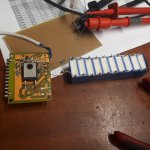
In the attached photo you can see how ridiculous my replacement diode looks!
The plan is to mount the lot in a small Hammond box, and heatsink the diode and FET to the box.
Next will be at add the 300k resistors, 10uF cap (22uF is far better ripple though) and diode for the other rail....
In the attached photo you can see how ridiculous my replacement diode looks!
The plan is to mount the lot in a small Hammond box, and heatsink the diode and FET to the box.
Next will be at add the 300k resistors, 10uF cap (22uF is far better ripple though) and diode for the other rail....
Attachments
Hi,
My theory is that the body diode of the FET is in conduction longer, due to slower reverse recovery from the diode on the secondary circuit and the coupling between windings
At the risk of being wrong...
If it is a simple Single Switch Isolated Flyback Convertor the FET body diode should never enter forward conduction and therefore your theory is wrong unless you can claim that the convertor has some concept of resonant mode operation.
Slower Trr on the output diode will hurt RdsOn dissipation on the primary FET if the convertor is operating with continuous current. The FET would have to drive that recovery. However leakage inductance would have to be extremely low for that to be a problem.
Since you have a scope maybe you can supply some pictures of the primary FET drain voltage and secondary Diode voltage, not bar end, both referenced to the appropriate grounds.
Try to do it zero ground lead. Someone else will have a picture but if you take the tit off your probe there will be a nipple and ground ring. You may have already lost the springy thing so you will have to improvise.
Haha my theory is based on guesses liberated from a tiny curriculum of buck boost supplies I studied at university.
The body diode should never conduct (I didn't know it should never conduct)
I learned something new
It is indeed a single switch boost, with push pull CT transformer secondary.
I can have a go at scoping the diode and FET (yes I see lots of bad press about ground clips, not sure a spring is a great idea at HV though)...I'll have to find a safe way
Last edited:
Soldered on 50/75ohm BNC.
Bike Forums get up tight about Free Wheel VS Free Hub so I will not mention Single Switch Flyback VS Boost or your Push Pull description of the secondary...
If the negative rail were to be implemented both the positive and negative rails would be supplied with power at the same time.
If you can get those waveforms, short ground, then I will take a guess there will be some serious ringing going on. Keep the probe on x10.
Please excuse my verbosity. The PSU has a centre tapped secondary for bipolar output.
It's frustrating to see CT used to mean centre tapped....
A CT is a totally different device altogether
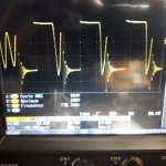
See attached waveform at diode anode, square wave excitation with several cycles of exponentially decaying 'ringing.
100V/div
5us/div
The FET measure will wait until tomorrow (clocking out time here in the UK)
It's frustrating to see CT used to mean centre tapped....
A CT is a totally different device altogether
See attached waveform at diode anode, square wave excitation with several cycles of exponentially decaying 'ringing.
100V/div
5us/div
The FET measure will wait until tomorrow (clocking out time here in the UK)
Attachments
Last edited:
Kodabmx I've also seen those and briefly considered it. The 20kHz square wave output scared me off, ok it's easy enough to rectify and filter out, but it's the EMI at 20k that worries me.
In the attached photo you can see how ridiculous my replacement diode looks!
The plan is to mount the lot in a small Hammond box, and heatsink the diode and FET to the box.
Next will be at add the 300k resistors, 10uF cap (22uF is far better ripple though) and diode for the other rail....
The transformer is different on the single sided output. The coil is smaller. I doubt it will work if you simply add the parts. I use 100uF on mine...
I use the one i posted in a phono preamp and there's no 20kHz on the output.
- Status
- This old topic is closed. If you want to reopen this topic, contact a moderator using the "Report Post" button.
- Home
- Amplifiers
- Power Supplies
- High Voltage Boost Converter - sacrilege?