homemodder said:...although I dont think it is required in the ltp nor those caps...
Those little caps help tame the local CFP loop. Lowering their
value below 5pf introduces a peak in phase response around
10Mhz, and raising the value above 12pf introduces a peak in
phase response around 20Mhz. Between around 5-12pf keeps
the phase response steady in that frequency range.
Also, even though the CFP looks balanced, it isn't. The PNP side
is biased at 1.4ma and the NPN side at about .6ma. This
ratio seems to produce the lowest distortion.
One more thing...to get mind numbingly low on distortion...
remove the 50 ohm emitter degen resistors from the LTP and
drop the NDFL cap to 50pf. The 0db point shoots out to 15Mhz,
but the distortion results improve by another 20db.
Square waves also still look great.
Which brings up a question I wanted to ask in general...
how do you know where to set the 0db point for loop
gain? I know it should be low because the NDFL feedback loop
encloses many devices.
jcx,
thanks for the PNG file.
mfc,
thanks for the PNG file.
mfc,
Why should it be balanced?Also, even though the CFP looks balanced, it isn't.
Not necessarily.The PNP side is biased at 1.4ma and the NPN side at about .6ma. This ratio seems to produce the lowest distortion.
Despite mind numbingly low distortion and great square waves, I`m expecting a rather poky sound of the present arrangement.One more thing...to get mind numbingly low on distortion... remove the 50 ohm emitter degen resistors from the LTP and drop the NDFL cap to 50pf. The 0db point shoots out to 15Mhz, but the distortion results improve by another 20db. Square waves also still look great.
Lumba Ogir said:I`m expecting a rather poky sound of the present arrangement.
I laid my cards on the table. How about showing yours?
Mike
mfc,
look, I don`t dislike the basic design but I would:
-use JFET for Q18/19 (important)
-remove C13/14 (very deteriorating), R48/54, C8, R30/31/32, C17
-change the VAS topology
-insert gate stoppers for M1/2 (important), base stoppers for the output transistors
to start with.
look, I don`t dislike the basic design but I would:
-use JFET for Q18/19 (important)
-remove C13/14 (very deteriorating), R48/54, C8, R30/31/32, C17
-change the VAS topology
-insert gate stoppers for M1/2 (important), base stoppers for the output transistors
to start with.
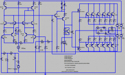
mfc said:
Its set at a little over 200ma thru each output transistor.
So class A at low signal levels, class B at higher.
I saw more problems using a bipolar output driver like the
MJE15034. This was harder to control. Using the ECX10N16
in this position was easier. Maybe this is a modeling issue?
If you are using the models from ONsemi then that would be it. Their MJE150XX models are particularly bad.
If you want to use MOSFET drivers then you will need to scrap the standard Vbe multiplier and use some type of nfb / bias-spreader circuit.
Cheers,
Glen
G.Kleinschmidt said:
If you are using the models from ONsemi then that would be it. Their MJE150XX models are particularly bad.
If you want to use MOSFET drivers then you will need to scrap the standard Vbe multiplier and use some type of nfb / bias-spreader circuit.
Cheers,
Glen
Please say more about a nfb / bias-spreader. Not sure what
the problem is or what that solves or what it is.
p.s.
Your moniker looks like she got up to early this morning and
didn't put on her makeup yet.

mfc said:
Please say more about a nfb / bias-spreader. Not sure what
the problem is or what that solves or what it is.
The problem is temperature compensation of the bipolar output stage and maintaining an emitter-emitter voltage of approximately 50mV with some degree of accuracy. I’m surprised that no one has mentioned this already.
You simply can't do that with a Vbe multiplier that gives a gate-gate potential of several volts for the MOSFET drivers.
Simplifying, suppose that a gate-gate voltage of 6V is required. The Vbe multiplier will have to be set with a multiplication factor of about 8. The Vbe multiplier will then have a temperature coefficient of about 17mV/deg C – massive overcompensation.
And on top of that you have variation of Vgs of the MOSFETs to contend with also. All you need is a Vgs variation of 1% and your EF OPS bias is all well and truly over the place.
A bias-spreader is a circuit that replaces the Vbe multiplier and servo’s the biasing voltage by monitoring the emitter-emitter voltage of the output devices.
Cheers,
Glen
Lumba Ogir said:Glen,
that man looks familiar, Father McKinsey, right?
No!
http://au.youtube.com/watch?v=2TQuacxEjAU
...
Simplifying, suppose that a gate-gate voltage of 6V is required. The Vbe multiplier will have to be set with a multiplication factor of about 8. The Vbe multiplier will then have a temperature coefficient of about 17mV/deg C – massive overcompensation.
...
Can you go even slower for me. In your example why does the
Vbe multiplier have to be set with a multiplication factor
of 8 and how does that give 17mV/deg C?
In this circuit, the gate-gate voltage is 1.7V to get
50mv on the emitters. This is smaller than if the drivers where
bipolars like 15034s - which would need 2.3V
Thanks,
Mike
Lumba Ogir said:
...
-use JFET for Q18/19 (important)
-remove C13/14 (very deteriorating), R48/54, C8, R30/31/32, C17
-change the VAS topology
-insert gate stoppers for M1/2 (important), base stoppers for the output transistors
to start with.
The first two look like an interesting alternative and simplification.
Using the JFET removes the need for C13/C14 R48/R54
and the bias circuit composed of R30/R31/R32 and C17. So far
I'm not able to get this alternative to produce a square wave in
simulation without oscillation. I'll look at it more and any
suggestions appreciated as to how to get it to not oscillate
are appreciated. I'm not sure if you are a simulation advocate,
but I take it you are not.
I think I'll leave the VAS alone for now.
Gate and base stoppers are probably something that is
needed practically speaking, but I left them out just to
simplify things.
Thanks for the feedback,
Mike
mfc said:
Can you go even slower for me. In your example why does the
Vbe multiplier have to be set with a multiplication factor
of 8 and how does that give 17mV/deg C?
In this circuit, the gate-gate voltage is 1.7V to get
50mv on the emitters. This is smaller than if the drivers where
bipolars like 15034s - which would need 2.3V
Thanks,
Mike
Woops. I just assumed a Vgs of a couple of volts for the example, thinking you were using Vertical MOSFETs.
The situation is a lot better for the Lateral devices you have chosen, but I can't predict how well it would pan out in real life, having never built and measure such a thing.
~6V / Vbe = ~8
8 * 2.2mV/degC = ~17mV/degC
Cheers,
Glen
Yeah this is definitely pushing the simulation envelope. ILumba Ogir said:mfc,
you should use JFET for every reason, preferably 2SK170 or some other type from Toshiba. I would not trust simulations too much, just implement it with 1-2 mA current, like many people have done.
trust simulators...just not the models.
This hobby is very conflicting. My right brain says the same
thing you do. My left brain does not. I kind of work out a
compromise between them.


Lumba Ogir said:mfc,
FET models are especially less reliable.
I would go for 4-5mA per side, around 5V across R39, K8C3503 for Q1/2.
made just those changes to the original circuit...
6db change for the worse in H3 at lower frequency (20Khz)...
about the same H3 at 100Khz...
but a 200Khz sine wave doesn't look like a triangle anymore.
It looks like a sine wave.
So way better somewhere above 100Khz. This may be audible
although it might be subtle I would think.
Mike
FET/BJT
Minimizing the coupling between stages with FETs could be
interesting.
So while losing about 10db on distortion, in real life this
might be worth looking into.
Each stage consists of a FET/Bipolar combination.
It works on square waves as well by keeping C13/C14 and
R46/R54. C13/C14 can be lower and are 4pf in value.
Has a certain aesthetic appeal to it.
If use a FET in the VAS, is it still considered a Baxandall super
pair? Maybe it doesn't really matter what we call it.
Attachments
hibias input
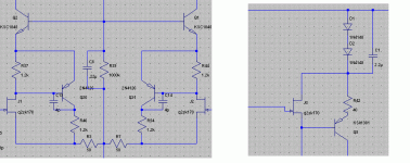
Lumba,
I did find success with hi-bias .008ma on the input,
slightly differently.
Attached is the circuit. It makes things more stable so
can eliminate the little local feedback caps needed at
.004ma. As well as the little lead compensation feedback
cap.
Mike
Lumba,
I did find success with hi-bias .008ma on the input,
slightly differently.
Attached is the circuit. It makes things more stable so
can eliminate the little local feedback caps needed at
.004ma. As well as the little lead compensation feedback
cap.
Mike
Attachments
- Status
- This old topic is closed. If you want to reopen this topic, contact a moderator using the "Report Post" button.
- Home
- Amplifiers
- Solid State
- hi-loop gain amp