Thank you for your information, but I don't fully understand your meaning
I worries about Ciss and linearity of those kind mosfets may cause bad effect to the hf sonic range.
BR
To answer your question more directly.
In a class A amp - with 3 gain stages, the IXFN 180n10 MOSFET sounded amazing.
For the n channel IXFN 180 n10 Ciss ~ 9.1nF
and the p channel IXTN 170 p10p Ciss ~ 12.6 nF
These MOSFET's are made using a single die - and the data sheet for the IXTN 170p10p says one application is for push pull amplifiers.
I'm no expert - but looking at the family of curves for the IXTN170p10p - the linearity looks OK.
But the real intent is probably for switching applications.
To point out, the IRF FB180sa10 looks to be the same, however, its made by internally paralleling MOSFET's.
The IRF version probably has matched MOSFET's, but there is no guarantee they are.
In an F5 style amp, I am very close to completing a design using these MOSFET's.
Beethoven Piano Trios and the Spin Doctors sound very good with it.
However, other guys on DIY Audio live and breath amplifier design.
I suggest you look at the F5 Turbo builder's form - and follow their experience.
http://www.diyaudio.com/forums/pass-labs/207103-f5-turbo-builders-thread.html
....
But I didn't like the idea of trying to match numerous IRF240 MOSFET's.
Then I had heard about how great the Gamut D200 mk3 power amp sounds and they used 2 power MOSFET's per channel.
So I prototyped this amp biased at 0.4 amps and it sounded amazing.
The current sources for the first 2 stages could be improved.
Without the current mirror the amp sounds warmer.
Output protection needs to be added.
However, a 30 watt class A amp is biased at around 3 amps.
It soon became clear the power dissipation was unreasonable.
The amp would dissipate 300 watts just in idle ... this would be a space heater.
BEFORE the Turbo F5 was released, I though I would increase the output of the original F5
by adding the IXFN180n10 power MOSFET's.
.
Ohh I see, now I get your "jaw dropping" meaning clearly

An externally hosted image should be here but it was not working when we last tested it.
In our location, it's hard and expensive to find matching numerous IRF240 MOSFET's, so that why I take my focus on your idear. I got IXTN15N100 and PM50502C from industrial PSU board. Can you help me prototype an amp with those mosfets.
Big thanks
Zen Mod,
I tried your follower buffer.
Got a bit nervous and used 100 R for the source resistors.
When the amp was switched on - BOTH voltage rails dropped from 25 v to 21.6 v - yikes !!!......
.
I forgot to ask previously - did you re-set bias to zero , prior to powering amp ?
Well Uunderhill,
I have neglected this thread, and it was good that I did so.
You have shown nerve and imagination, and ZM and Jacco are merely
testing your resolve.
You are nominated to cadet-leader rank in Fearless Amplifier Builders.

Thanks for your support and promotion - its not easy being a member of FAB.
I wasn't afraid of making a mistake tinkering with amp designs.
Its the Hazing I got that scares me.
.
Ohh I see, now I get your "jaw dropping" meaning clearly
In our location, it's hard and expensive to find matching numerous IRF240 MOSFET's, so that why I take my focus on your idear. I got IXTN15N100 and PM50502C from industrial PSU board. Can you help me prototype an amp with those mosfets.
Big thanks
Yes - jaw dropping in audio terms means - the sonics are surprisingly good.
I checked a data sheet and the IXTN 15N100 is an N channel MOSFET
designed for high voltage switching applications.
The Hitachi PM50502C is also an N channel - however, a family of curves is shown on the data sheet.
Looking at these curves, it appears the linearity of this device seems to be fine.
Vds (max) = 500v
Id = 50 A @ what temp ?
Rds(on) = 0.09 ohms
Ciss = 10.3 nF
Vgs(on) = 1.5 to 4 v
gm = 40 A/v typical
The Hitachi PM50502C is the device to use.
There are actually 2 MOSFET's on each device.
You would need to find a design that uses N channel MOSFET devices only.
You could use the schematic for the class A amp I prototyped above
but bias it at around 1 amp to make a 10 watt amp.
The current sources really should be improved and output protection added.
This would make a fabulous amp - but you would need heat sinks.
.
I forgot to ask previously - did you re-set bias to zero , prior to powering amp ?
Everytime I tinker with a change, the trimmers get set back to 0 - and the amp gets re biased.
Quite frankly, I would have done it old school - used a source follower with a current source.
However, as you previously suggested - I lowered the source resistors for Q1 and Q2.
Actually, I've even lowered them more to 3R6.
I've tried paralleling up Q1 and Q2 - and can't hear any difference between 3 and 4 jFET's paralleled* up.
Which says 3 paralleled jFET's are providing enough poop for the "bricks."
So I'm sticking with 3 paralleled jFET's for Q1 and Q2.
Also, I've tried lowering the gate resistors for the "Bricks" to reduce t = R * Ciss.
However, the FB loop will start "singing" (oscillating) if the gate resistors are lowered.
Actually, I'm going to try setting R * Ciss to be the same for both power MOSFET's.
Don't know if that will make any audible difference.
*Info on jFET temperature coefficients seems to be non existent on data sheets.
However, for a jFET, the gm decreases with an increase in Temperature.
Also, the channel resistance increases almost linearly with an increase in Temperature.
So thermally speaking - 3 paralleled jFET's should be happy together.
Here is a read on paralleling devices.
http://web.eecs.utk.edu/~tolbert/publications/apec_2011_madhu.pdf
.
Your transconductance is so high that Ciss probably is not your issue.
Crss at 1600 pF looks like 5K ohm at 20 KHz, so you will have to source
1 mA into the Gate for every 5 volts you want to swing. This probably
will just work with a single pair of 2SK170/2SJ74, but you certainly can
do better with as many as 4 in parallel.
Crss at 1600 pF looks like 5K ohm at 20 KHz, so you will have to source
1 mA into the Gate for every 5 volts you want to swing. This probably
will just work with a single pair of 2SK170/2SJ74, but you certainly can
do better with as many as 4 in parallel.
Papster is just testing your resolve.
I appreciate the input from everyone.
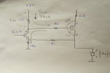
Here is the simplification of the prototype - there is plenty of poop to drive the "Bricks."
Today I read up on Miller capacitance, Gate Charge curves and all sorts of stuff
but IMO its the 0.5 source resistor that is holding this amp back.
.
Attachments
Notes
Big E has christened the F5 with Gamut style MOSFET's as the "G5."
With N.P. discussing Cgs and a high transconductance, I looked up the Miller effect,
but I think I'm spinning my wheels on this issue.
Cin = Ciss + [ 1 + Av ] * Cgd
I remember an old IRF application note from the 1980's - where they showed building audio amp using HEXFET's.
Usually, the old application notes are great, but this one was disappointing.
http://www.irf.com/technical-info/appnotes/an-948.pdf
With the "Bricks" its almost like you need learn about them in a switch mode application and then transfer that knowledge to analog.
Turns out in switching applications, they are often driven by push-pull BJT's.
However, I can absolutely say - a resistor and a 2n2907A will drive the gate just fine.
Other people on DIY Audio have looked into cloning the Gamut D200 MKiii
http://www.diyaudio.com/forums/soli...h-pull-pull-like-gamnut-whats-right-name.html
http://www.diyaudio.com/forums/solid-state/192173-poweramp-irfp4668.html
I don't have any power resistors - to create a load - and measure the voltage drop in Vout - and then plot a load line to get Zout.
However, again, I think its a high Zout that is holding the "G5" back.
.
transfer function
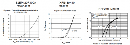
I may be mistaken, perhaps the fact that two of these graphs are linear and the last is logarithmic is tricking my eye, but all of these IXYS HiPerFETs seem to have a transfer function which is more like that of a JFET. This may have something to do with the alleged amazing soundingness (not a real word) of this Mosfet. This seems the same for smaller Mosfets, like the ones in TO-247 packages, in the HiPerFET family. I guess you could drop it into an Amp Camp amp without any other modifications to see if it has promise in that circuit as well. It has 1k ohm from gate to source with a single 2SK170 in follower mode. I have always wondered about the 2SJ109 in the J2 if some trick is needed to make the JFETs share the load. There don’t seem to be any source resistors perhaps the fact that there are two matched 2SJ74 is sufficient to make them share the load relatively equally.
Disclaimer – I am not looking to build an F5, I may build an amp camp when the PCB comes out.
Attachments
Please bare with me - its been more years than I care to admit, since seriously looking at analog.
I've been trying to find an equation that describes |Zout| of the F5.
for a MOSFET
r out = 1/ (lamda * Id) = 1/gds = d Ids / d Vds
that's great - but without a family of curves how do you get d Ids / d Vds ?
For the F5
Zout = Rs + 1/gds but there are 2 output stages and also F.B.
so I think |Zout| = (Rs + 1/gds) / (2 * F.B.)
Is this right ?
.
Last edited:
without curves and specific data , it's inevitable that you must do some measuring
so - either measuring xconductance of mosfets (Papa's papers 0n FW site - Mosfet Testing ) or measuring output impedance directly
for last one , to save my fingertips , just click on this :
info and calc : Output Impedance
online Java calc : Measuring input impedance and calculating output impedance calculation calculate amplifier amp total loudspeaker speaker microphone resistance resistor bridging matching test load loudspeaker source resistance - Why input impedance is in parallel and
For a stage with a high output impedance without feedback (F5 qualifies),
you can estimate output Z by dividing the loop gain into 8 ohms by the
open loop gain (also into 8 ohms) and multiplying by 8 ohms.
Example: Closed loop = 10X, Open loop = 30X
10/30 X 8 ohms = 80/30 = 2.66 ohms
If you can't measure the open loop, then estimate it by the ratio of
Output load / (1/transconductance + degeneration)
Example for single stage:
Transconductance = 2 amps/volt = 2 Siemens
Degeneration = 0.22 ohms, Load = 8 ohms
Gain = 8 / (1/2 + 0.22) = 8 / 0.77 = 10.4 X
Cascaded stages are simply calculated separately and then multiplied.
Let's take the F5 as a specific:
Input Fet = .04 S, Degen = 10 ohm, Load = 500 ohms
Gain = 500 / (1/.04 + 10 ) = 500/35 = 14.3
Output Fet = 3 S, Degen = 0.47 ohm, Load = 8 ohms
Gain = 8 / (1/3 + 0.47) = 8/.8 = 10
So the gain of either the top or bottom half of the complementary
circuit is about 14.3 X 10 = 143
Since this circuit has two halves contributing ( + and - half), multiply this
by 2. As a ball park, the open loop gain would be 286X
If the loop gain is 15 dB (about 5X) then we have about a 57 X ratio
between open loop and loop gain, so the thumbnail estimated output
impedance is about 8/57 = 0.14 ohms, which comes out about right.

- Home
- Amplifiers
- Pass Labs
- Help with F5 with Gamut style MOSFET's