Pierre,
I will make up the new inductor tomorrow. I will use several strands as you suggest. I have done this before in SMPS transformers.
Was just thinking about your comment about effecience / heatsink size.
It the head sink rises by 10 deg in 1 hour and its cooling capacity is about 0.5 K/Deg then my fets are dissipating about 20Watts... Not bad considering I am getting out say 600 watts for that entire time.. This only accounts for a 3.3% loss I can live with that.
Of course I am not stating that the amplifier is 96.7% effecient I am just commenting on losses in the switching FETS.
Regards
Peter.
Well, the good way to measure efficiency is to connect a true-RMS multimeter in series with one of the rails, measure RMS current, multiply with the voltage (you have another voltimeter in the supply input of the amplifier measuring ACTUAL voltage) and all this is done while you measure the output in the load. It is important to measure all things at the amp leads, as you can have some watts dissipating in the wires!
For higher powers (<50W or so), although the negative rail consumption is a bit higher due to the driver IC supply, you can roughly consider that the Vcc and Vss currents are the same, so measure Vcc and to calculate consumed power,
Pcons=2 x Vcc x I(rms)
At the load, Pload=Vout(rms)^2 / Rload
This afternoon I will measure efficiency of my amp and study variation with the gate resistors and dead-time.
Hope to hear from you soon,
Pierre
Hello Pierre,
I have just done some prelimary effeciency measurements.
I measured the Input Current with a True RMS current meter on the V+ Rail
The output Cycle RMS voltage was calculated by a Tektronics TDS220 Digital Scope.
I really need a better power supply by the way. Each rail drops up to 20V under large continous loads, ie Sine Wave as tested with. I am going to buy a 1000VA 55-0-55 Torroid i think. Currently its only running off a 300VA 50-0-50, however I have been over driving it with my variac, 55-0-55. I have also paralled a second one in series for the higher power longer runs.
The following are 3 different sets of measurements, the amplifier is not really running at a very high power level this can be seen from the output RMS voltage..
Because of the supply ripple (100Hz) It is hard to get a stable reading for the I-in. so there is a little bit of error in that.
Test 1
Freq Out = 500Hz
Vin = 62.6 Rail
Iin = 2.33 RMS
P In = 291W
Vout RMS = 28.3v
R Load = 2.8 ohms
P Out = 286W
Effeciency = 97%
Test 2
Freq Out = 1000Hz
Vin = 68.1
Iin = 2.24
P In = 305W
Vout RMS = 28.6
R Load = 2.8 ohms
P Out = 292W
Effeciency = 95%
Test 3
FreqOut = 500Hz
Vin = 62.0
Iin = 2.5 A RMS
P In = 310W
Vout RMS = 29.1V
R Load = 2.8 ohms
P Out = 302W
Effeciency = 96%
Regards
Peter
Yesterday I was also doing some efficiency measurements.
On 2.65 ohms load, and discounting the modulator's and driver power consumption, thus only taking into account the output stage losses, (mosfets and filter) at 262W output efficiency is about 91.5%.
I think that most of these corrersponds to switching losses (total conduction losses are Iout(rms)^2 * Rds(on), right?)
I will try to increase the gate drive voltage from 12V to 15V, that should speeed up transitions, and perhaps decrease frequency a bit, from 285KHz to 230KHz or so.
I attach a photo of the gate drives, now that the gate resistors are 6 ohms instead of 10. I have noticed almost no difference, so I don't know how to speed up the switching more. It seems that the rise/fall times are too long. The mosfet has 110nC max. gate charge, 3200pF máx total input capacitance.
Peter's mosfets are larger and he seems to be getting higher efficiency. What can I do to improve switching times apart from using lower gate charge mosfets?
Thanks!
Attachments
Hi,
I made the inductor i was talking about, 26 turns on a powdered iron core, to give approximatly 30uH. I used 4 strands of 0.9mm wire twisted together. My Bypass capacitor was 330nF.
However the thing get so damn hot, not the core just the windings. I guess i need more inductance?? Also the output ripple has jumped from less than 1v pp to about 15v pp.... I hate to think how much extra EMI there is now.
Any suggestions??? Should i try a different core. I have some Large ETD59 `E' Cores with bobin, however I would prefer not to use them as they are too big for this circuit board, and hence would much prefer a toroid.
Regards
Peter.
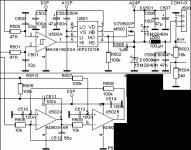
Yesterday I accidently shorted the output terminals of the amplifier ( A really dumb thing to do.) anyway it killed the output fets and driver IC. So i have decided its time for over current, and also supply pumping / over voltage protection.
After looking at a few reference designs this is what i am thinking, can anyone point out any problems with the design so far..
The ir2110 has a SD pin, once pulled high the driver IC turns off.
I have a RC network feeding the SD pin of the 2110 in order to reduce spurious shutdowns, is this a good idea? do i need a larger or smaller time constant??
I have attached a pdf file of the anticipated changes. Note: lots of information has been left off this schematic.
Any suggestions / help is much appreciated
Regards
Peter
Attachments
About the inductor, it shouldn't get too hot, less with 4x0.9mm, something is wrong there.
And the ripple shouln't be so high. If you tell me the sw. frequency, the supply voltage and the load resistor you tested with, I can calculate for you the ripple you should have assuming that the 30uH value is correct. Have you measured it? I suspect it has not thet inductance.
About the protection circuitry, I see you are basing on what IR reference design does.
I assume that D1, D2 and D3 form a overvoltage protection also. When the PNP is activated due to overcurrent, it passes current to D4 so it biases and activates SD pin.
I think it is easier to sense the current in the negative rail, so you have all the grounds referenced to the negative rail, and you don't need zeners at all: for example, use a NPN instead of the MJE350, with a collector resistor to the driver's supply (Vss+12v), and emitter to Vss. The output of that transistor (collector) should go low when overcurrent is detected. Then you can invert that with another transistor and attack SD pin.
In any case, I would include a time constant (as you have done, although somewhat longer), so when overcurrent is triggered, SD pin is high for about 1 second or so.
Please keep us updated!
I have discovered problems with my feedback scheme (after filter), please read the other thread, as this can affect you if you finally go for that also.
My switching frequency is 250kHz, supply voltage +/- 80V Load resistor 2.5Ohms
Yep D1,D2 D3 are for over voltage protection. I think it is actually easier to current sense in this application from the + rail. Given that I would need the string of Zener diodes for the over voltage protection its just easier to tap a pnp in where i have
Regards
Peter
Yep D1,D2 D3 are for over voltage protection. I think it is actually easier to current sense in this application from the + rail. Given that I would need the string of Zener diodes for the over voltage protection its just easier to tap a pnp in where i have
Regards
Peter
Well, following my simulations, you should have 29.5dB of attenuation at 250KHz, that means that the ripple should be about 5.36Vpp at +/-80V rails.
If all the other componentes are as you say, 330nF and 2.5 ohms, to get 15Vpp of ripple with +/-80V rails you should have about 10uH of inductance instead of 30uH.
I think you have miscalculated the number of turns of your coil, but I can have missimulated, too ;-)
About the protection, your approach can be good, too. If you implement it, tell us how it goes. I would short the output and start increasing the input voltage until it engages. It should act quick enough and then remain in shutdown mode for a while. This is how I like it, at least.
Hope this helps.
")
Hi,
Up until now I have used my Function Generator to supply the 250kHz triangle wave that i use for my comparator to generate the PWM.
What is the best ( or at least good) way to generate a clean triangle wave.
I was thinking a Intergrator / schmitt triger setup with two opamps. I have done this in the past, however at 250kHz the output it quite distorted. I was using a TL072. Can anyone suggest a better opamp for this??
Or Maybe should i try making the system not carrier based.
Regards
Peter
At that frequency you won't do with a TL082.
You have several alternatives:
1) Use a MAX038. Very good linearity
2) Use a fast double opamp, like Lf357
3) Use a oscilator module, divide it with a digital counter and then use a opamp integrator, again as fast as possible.
I use a MAX038 with very good results.
Hope it helps,
Pierre
You have several alternatives:
1) Use a MAX038. Very good linearity
2) Use a fast double opamp, like Lf357
3) Use a oscilator module, divide it with a digital counter and then use a opamp integrator, again as fast as possible.
I use a MAX038 with very good results.
Hope it helps,
Pierre
Just another quick question,
Is there any reason why a triangle wave is better for PWM than a Sawtooth???... I can generate a very nice sawtooth waveform at 250kHz using a const current source and a 555. Where as a nice clean triangle wave is a lot harder, I don't really want to use and opamp intergrator, I also don't want to use a Function generator IC, They are $40 ea here.
Regards
Peter
I understand that you want to avoid IC's, but if you are going to build the amp for your own use, you can very easily order MAX038 samples from maxim, for example.
About the sawtooth, I think there is no problem with it theoretically, but I don't know what the fall time of it can be as a maximum for proper performance.
Best regards
BTW: Peter: don't you sleep?? ;-)
About the sawtooth, I think there is no problem with it theoretically, but I don't know what the fall time of it can be as a maximum for proper performance.
Best regards
BTW: Peter: don't you sleep?? ;-)
Hi,
I used a two channel synchronised(!) triangle version, not for audio, but for a fast heater control.
Minor changes from the schematic:
- 100nF before R506
- C510 1nF
- C512 150pF
- 100k parallel to C512
Major disadvantages:
- hard to get the triangle stable, moves around the average value. Could minimise it, but not remove completely. Maybe better with a freerunning generator.
- poor linearity and correlation between input and output voltage
- MAX 942 cannot work with high differential voltages due to its triple antiparallel input protection diodes, resulting in low possible triangle amplitudes
- restricted modulation factor (~15%...~85%)
I will switch to a self oscillating design, similar to one, Bruno suggested to me sometimes. This will incorporate a overall feedback.
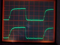
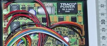
In the photo the comparator is under the "wire crossing", the generator is rightt of it. Power stages are in the upper left, using all SMD and remaining cool under all circumstances (at least one good thing) .
.
Somewhere it was written, that the MAX038 is not well suited for audio purposes due to its nonlinearity and noise at these frequencies, did I misunderstand that?
My experiences with a sawtooth was the hard to realise steep shut off edge without spikes. The discharging switch (BJT or FET) injects charges into the circuit, resulting in negative overshoot. I realised it with an open drain HC03 switch (at ~600kHz) a couple of years ago.
Regards, Timo
I used a two channel synchronised(!) triangle version, not for audio, but for a fast heater control.
Minor changes from the schematic:
- 100nF before R506
- C510 1nF
- C512 150pF
- 100k parallel to C512
Major disadvantages:
- hard to get the triangle stable, moves around the average value. Could minimise it, but not remove completely. Maybe better with a freerunning generator.
- poor linearity and correlation between input and output voltage
- MAX 942 cannot work with high differential voltages due to its triple antiparallel input protection diodes, resulting in low possible triangle amplitudes
- restricted modulation factor (~15%...~85%)
I will switch to a self oscillating design, similar to one, Bruno suggested to me sometimes. This will incorporate a overall feedback.
In the photo the comparator is under the "wire crossing", the generator is rightt of it. Power stages are in the upper left, using all SMD and remaining cool under all circumstances (at least one good thing)
.Somewhere it was written, that the MAX038 is not well suited for audio purposes due to its nonlinearity and noise at these frequencies, did I misunderstand that?
My experiences with a sawtooth was the hard to realise steep shut off edge without spikes. The discharging switch (BJT or FET) injects charges into the circuit, resulting in negative overshoot. I realised it with an open drain HC03 switch (at ~600kHz) a couple of years ago.
Regards, Timo
Attachments
Triangle or sawtooth:
http://www.diyaudio.com/forums/showthread.php?s=&threadid=26670&perpage=10&pagenumber=1
Triangle is better, both are flawed, simple work around.. self oscillating.
Timo, SODA or UCD?? SODA is inferior in alot of ways. More than one picture in same post... only way I know is to zip them.
Regards,
Chris
- Status
- This old topic is closed. If you want to reopen this topic, contact a moderator using the "Report Post" button.
- Home
- Amplifiers
- Class D
- Help with Class D Amplfier Design (feedback)