Thank you for the screenshots! I feel like I am right on the cusp of understanding.
I do believe that I have a transformer I will be able to use for an isolation transformer. Unfortunately I do not yet own a variac. It is one piece I absolutely know I need, but since most of my work is 12Vdc and I have a 50a current limiting transformer isolated 12V supply, I have always pushed that purchase off to "someday". I may just break down and order one. I'll look into it this afternoon.
I do not have a high voltage probe, but I believe my my scope's max vertical range is 50v/div, and the inputs are rated for +-300V. I think I should be able to get the primary side waveforms with a 10x probe.
I will make this a priority on my next day off (next Friday-- shift worker here and am buried under overtime at the moment). Thank you for your continued patience.
Thanks,
Jason
Hi, I did not get as much time as I had hoped today. My wife took my girls school shopping, so my son stayed with me and wanted to build lego robots...
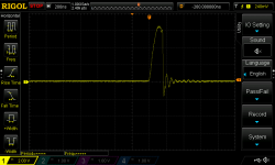
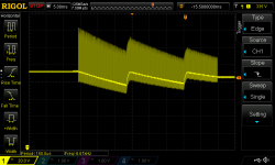
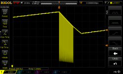
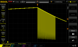
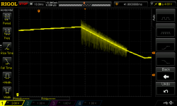
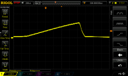
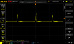
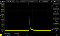
Anyhow, I talked him in to hanging out in the shop for a little while. I reinstalled the transformer and I tried to get the requested waveforms. I can try again if I still did not get enough detail. They are all still referenced to PG, but I adjusted the zero level to get as much detail as possible in the screen shot. I assume that the waveform detail is more important at this point than knowing the exact voltage of the peaks. The waveforms on Vdd-g and Vdd both had zero set at approximately -9V. The waveforms captured on the drain terminals was with the zero at -330V.
Current Sense

Feedback

Drain

Drain 5ms

Hopefully this will give the information needed. If not I should have the day off sunday and with any luck will be able to get some time alone to do a little better job getting the new traces.
Thanks,
Jason
Anyhow, I talked him in to hanging out in the shop for a little while. I reinstalled the transformer and I tried to get the requested waveforms. I can try again if I still did not get enough detail. They are all still referenced to PG, but I adjusted the zero level to get as much detail as possible in the screen shot. I assume that the waveform detail is more important at this point than knowing the exact voltage of the peaks. The waveforms on Vdd-g and Vdd both had zero set at approximately -9V. The waveforms captured on the drain terminals was with the zero at -330V.
Current Sense
Feedback
Drain
Drain 5ms
Hopefully this will give the information needed. If not I should have the day off sunday and with any luck will be able to get some time alone to do a little better job getting the new traces.
Thanks,
Jason
Attachments
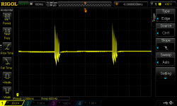
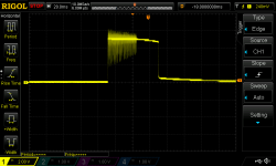
The narrow 200ns current sense pulse is indicating premature termination of pulses due to current limiting due to a short in the power path somewhere, or improper current sense resistor value (like 10 times bigger). CS pulse should look like rising sawtooth lasting longer than 200ns.
Thanks Eva!
I replaced the current sense resistors. There were 5 x 10R in parallel according to the schematic. That give a 2R value for the current sense resistor. I did measure the resistance of the whole group at the CS pin to ensure no open traces and that I got close to 2 ohms and my meter read just over 2 ohms. I did think that 2 ohms is rather high for a current sense resistor though. What are the chances that these were supposed to be 1R, not 10R... The originals were much to badly burned to read. I will see if I can find them on the bench though and see if I can clean one up enough to read it.
It looks like there is a possibility that if D910 were bad it might cause high current on the primary side. I have checked D910 in circuit, but I think at this point I should remove it from the board and make 100% sure.
I also have R935 lifted right now to take the secondary low voltage supply out of the equation. R935 supplies VCC to the ICE2b365 via D920 from the bootstrap (is that the right term? The small second primary side winding) winding on TF91.
Thank you again for your assistance! I'll reply as soon as I have any more findings to share.
Jason
Ok, I think the results are in...
I checked D910 yet again, this time out of circuit, it tested good.
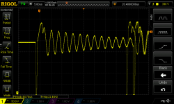
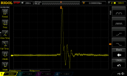
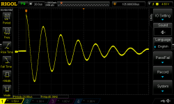
I proceeded to attempt to coble together a "ring test" from various sources online. I think that the results show that the transformer is bad. Am I interpreting this correctly?
First waveform is a known good SMPS transformer. 1kHz square wave fed through a 10nf poly cap (in series) with the scope across the same winding. When I short any other windings on this xformer, the ringing drops to 1-2 cycles and the amplitude drops dramatically.

Second is the Harmon Kardon transformer in the exact same setup. Shorting any other winding on the transformer changes nothing. I get a few more cycles from the ring if I check the bootstrap winding instead of the primary, but overall, it's far more dampened than the known good xformer.

So, am I contacting Harmon international tomorrow? If they will not supply parts, do any of you have any suggestions? I am not opposed to rewinding the transformer if it is possible to do by hand.
Thanks for all your help!
Sincerely,
Jason
I checked D910 yet again, this time out of circuit, it tested good.
I proceeded to attempt to coble together a "ring test" from various sources online. I think that the results show that the transformer is bad. Am I interpreting this correctly?
First waveform is a known good SMPS transformer. 1kHz square wave fed through a 10nf poly cap (in series) with the scope across the same winding. When I short any other windings on this xformer, the ringing drops to 1-2 cycles and the amplitude drops dramatically.
Second is the Harmon Kardon transformer in the exact same setup. Shorting any other winding on the transformer changes nothing. I get a few more cycles from the ring if I check the bootstrap winding instead of the primary, but overall, it's far more dampened than the known good xformer.
So, am I contacting Harmon international tomorrow? If they will not supply parts, do any of you have any suggestions? I am not opposed to rewinding the transformer if it is possible to do by hand.
Thanks for all your help!
Sincerely,
Jason
Attachments
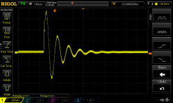
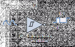
What is generator source impedance? The transformer looks shorted unless drive impedance is too high, or the ringing is from breadboard layout (is the other transformer from a flyback or what? which size?) If you have an adjustable frequency generator with say 50ohm output, you can find a frequency and a capacitor value allowing to pass something between square and sine wave through the transformer. Remember a LC resonates at Fr=1/(2*3.1415*sqr(L*C)). At 50~100khz it should draw low enough current to pass a 5V square wave from logic gates, maybe buffered with emitter followers, with series resistor and capacitor. These transformers are made to be driven fast.
The "bias" or "bootstrap" winding is usually employed as a shield too, so it is less coupled to the other windings, as it usually has to pass far less current.
Of course you can rewind it, critical process is cooking the transformer to 100C or so and separating the cores, applying heat to the cores or boiling it. This depends on the type of glue used, in consumer electronics often just the varnish is used as core glue. When disassembling the windings it's important to take pictures and/or notes so that nothing is missed when rewinding, including amount of layers of tape (3 required between primary and secondary, every time one is on top of another). It probably has 3mm margins at the sides that have to be respected, for 6mm creepage.
Last edited:
My honest answer is, I don't know. I'm using the function generator built into the inexpensive transistor tester. I tried to use the test output on the oscilloscope, but I don't think it can drive enough current, it would basically flatline after the first time it "rang". I'll try to find out the specs of the tester and let you know.
As for the other transformer, it was part of the smps from an old monitor. I don't know for sure if it is flyback design. I don't really think so. I just had company show up, but I'll respond more later. Thank you for taking a look.
Jason
As for the other transformer, it was part of the smps from an old monitor. I don't know for sure if it is flyback design. I don't really think so. I just had company show up, but I'll respond more later. Thank you for taking a look.
Jason
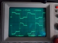
The pictures show a good transformer under raw test with no other equipment than oscilloscope, bench supply and breadboard:
- A 74HC14 hex schmitt-trigger inverter gate used as oscillator in a breadboard, powered with 5V, with buffered output. Recycled from another test. About 500khz.
- PNP/NPN emitter followers with 1k base drive and 47r output, clamping diodes, 100nF series capacitor on other end of primary. This produces a funny waveform as amplitude is so small that the conduction of the clamp diodes and NPN/PNP followes is clearly seen as diode drop.
- Primary being excited with nearly square wave, showing good symmetry from circuit and very little power/current drawn from transformer (current is a triangle wave).
- Top wave: CH 1, 10:1 probe, 500mV/div, measured at +12V secondary, grounded center taps of all windings, 10:1 probe.
- Bottom wave: CH 2, 100:1 probe, 2V/div, measured at primary, capacitor in series with other end of primary to provide a centered AC potential.
btw: This piece of breadboard is nearly 15+ years old and shows some learning errors from a long time ago, but was the more suitable one.
Attachments
Last edited:
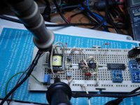
Eva, I did not get a lot of time in the shop today, my daughter wanted to spend some time with me so we vegged out together most of the day. It is going to take me a little time to digest everything in your prior post. I know I have a tube of 10 or 20 Schmidt trigger hex inverters. I should have all the other necessary components too.
I could not find published data on the output impedance of that small function generator. I followed some inductions online to measure it. The instructions were to measure the p-p voltage on the scope, and then add parallel resistance until you get to 1/2 of the original p-p. This should give a close estimate of the source impedance. The little atmega tester measured at 806R. I thought I would verify this method using my scopes probe compensation output, and it resulted in 11.8K. I looked through the rigol specs to verify my test results, and... The impedance is not published...
I will find time for more testing soon. I still have the next few days of work.
Thank you,
Jason
I did not have all the parts to build the oscillator. I have some non inverting CD4050 buffers, and some schmidt trigger inverting open collector SN7407N buffers, but not the ones in your test rig.
I decided to call Harman/Kardon to see if I could order the transformer. My thinking is that even if I was unable to properly test it, that by process of elimination it is really the only thing left. It was a bit under $15 shipped, so if it is not the issue, it wasn't a terrible expense.
I will post back when I get the new transformer and let you know if it was indeed the issue or if I have some other gremlin.
Thanks,
Jason
It's a matter of loading the 7407 open collector with 1k, buffering with 4050, taking the feedback from that 1st 4050, then using another 4050 to get the output (being perfectionists). I recommend you to build the little oscillator even with the part on order.
EDIT: Looking at datasheet I'm not sure the 7407 is a schmitt trigger, so it may not be so suitable for an oscillator, but it is TTL so not much trouble: supply current is under control even if the input is keep static at a level in the middle between low and high, unlike CMOS. Hysteresis can be added by means of a resistive divider between the junction of the RC and the input, fed by the output of 1st 7407 inverted back by another 7407 and maybe buffered by another 4050 for symmetry, this being fully perfectionist. These gates are hex.
EDIT: Looking at datasheet I'm not sure the 7407 is a schmitt trigger, so it may not be so suitable for an oscillator, but it is TTL so not much trouble: supply current is under control even if the input is keep static at a level in the middle between low and high, unlike CMOS. Hysteresis can be added by means of a resistive divider between the junction of the RC and the input, fed by the output of 1st 7407 inverted back by another 7407 and maybe buffered by another 4050 for symmetry, this being fully perfectionist. These gates are hex.
Attachments
Last edited:
Eva, I am getting a parts order together for some other repairs and projects I have going on, so I am just going to order a few of the 74HC14 inverters that you suggested earlier. My open collector inverters are actually slated for another project, and interface board for my big CNC mill, I know i don't have to leave the oscillator together permanently, but it seems like a handy little gem to have at your disposal.
That said, there have been more than a few times that I have wanted an arbitrary function generator for testing. I normally get by with a sound card based one for audio frequency stuff, but I'm thinking of actually buying a real instrument. I do not want to spend a bunch of money, I am kind of considering this inexpensive unit on ebay, JDS-6600, it is not badly priced for $85 for the 8Mhz model, and the specs seem decent. Probably the majority of my work will utilize it in the lower end of it's frequency range. I'm thinking that for how long I have been getting away with cobbled solutions, that this may be perfectly adequate for my needs. Aside from that, I am thinking about the base Rigol model, I am quite happy with my Rigol scope, but the Rigol function generator is significantly more money. I would also entertain any recommendations of an older used model to look for, but I think it is time I do something about this.
Thank you again for all of your time.
Jason
Good to have some 74HC14 for prototyping.
Good to have a signal generator, specs look suitable, 50r output impedance, 10~20Vpp output range depending on mode, accurate. For my work I would pick at least the 25Mhz model (+$13) since sometimes I have to analyze resonances in the 10Mhz~20Mhz range (paralleled capacitors in PCBs, transformers), I do R&D. The 8Mhz model could be adequate for repair and breadboard work.
Good to have a signal generator, specs look suitable, 50r output impedance, 10~20Vpp output range depending on mode, accurate. For my work I would pick at least the 25Mhz model (+$13) since sometimes I have to analyze resonances in the 10Mhz~20Mhz range (paralleled capacitors in PCBs, transformers), I do R&D. The 8Mhz model could be adequate for repair and breadboard work.
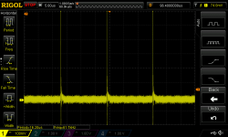
I'm pleased to say that I have the receiver back up and running. I bought the function generator I posted about earlier. I re-ran the same test I did on the old transformer with new function generator and on both the new and old transformer.
I also have the waveforms of the functioning power supply in case it will help someone else.
Thank you all so much for your help. It was a bit of a long road, but I am glad it is up and running again.
Sincerely,
Jason
I also have the waveforms of the functioning power supply in case it will help someone else.
Thank you all so much for your help. It was a bit of a long road, but I am glad it is up and running again.
Sincerely,
Jason
Attachments
-
 OB-drain_new_xformer.png47.2 KB · Views: 51
 -
 OB-FB_new_xformer_200ns.png36.3 KB · Views: 39
 -
 OB-FB_new_xformer_5us.png47.1 KB · Views: 45
 -
 OB-CS_new_xformer_200us.png33.1 KB · Views: 130
 -
 OB-CS_new_xformer_5ms.png33.7 KB · Views: 141
 -
 New_xformer_1khz_ring.png40.2 KB · Views: 136
 -
 old_xformer_1khz_ring.png38.9 KB · Views: 151
 -
 20170802_151159-picsay.jpg415.7 KB · Views: 61
Great work. You have completed 1st course in off-line SMPS repair.
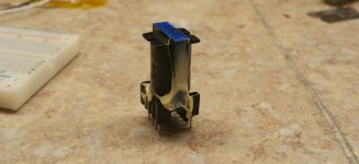
Old transformer is shorted, you can dismantle it to find out about the nature of the short.
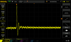
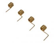
When capturing CS waveform I think you are measuring something else, bigger signal, superimposed, giving that LF repetition rate, like voltage drop of half rectified mains across some ground trace, and/or LF burst mode taking place. The actual CS waveform are the little glitches in the 200us/div capture, these are synchronized with switching waveform, and may not be cleean sawtooth, particularly at such a low load level. Low voltage <1V signals are tricky to measure in SMPS, close connection of ground and tip near circuit nodes is required (and preventing probe ground wire loop from picking up magnetic fields such as from transformers), like soldering a ground connection at some strategic point and laying out ground wire for low inductance (loop area), or bypassing probe ground wire with piece of wire (a ground tip) tied around the ground ring in the tip side of the probe (see attached image, when I use that gadget I do with plastic insulation from fine wire, so that only tip could do a short, already had some accidents with that). This requires some practice, ground tip slip can do a lot of harm.
FB pin is mostly DC, what you have captured, in the sub-volt level, is EMI interference from own power supply. Switching waveform looks OK.
I'm going to make two last recommendations for this receiver: Insert 10r 2W wirewound fusible resistor between the junction of (D901,D902) and C902:+ (R926 preferably connected after the 10r). Add 390V MOV (same size or bigger than nearly-dummy VT91) from AC-L to AC-N. This improves line surge protection and reduces damage in case standby supply fails.
Old transformer is shorted, you can dismantle it to find out about the nature of the short.
When capturing CS waveform I think you are measuring something else, bigger signal, superimposed, giving that LF repetition rate, like voltage drop of half rectified mains across some ground trace, and/or LF burst mode taking place. The actual CS waveform are the little glitches in the 200us/div capture, these are synchronized with switching waveform, and may not be cleean sawtooth, particularly at such a low load level. Low voltage <1V signals are tricky to measure in SMPS, close connection of ground and tip near circuit nodes is required (and preventing probe ground wire loop from picking up magnetic fields such as from transformers), like soldering a ground connection at some strategic point and laying out ground wire for low inductance (loop area), or bypassing probe ground wire with piece of wire (a ground tip) tied around the ground ring in the tip side of the probe (see attached image, when I use that gadget I do with plastic insulation from fine wire, so that only tip could do a short, already had some accidents with that). This requires some practice, ground tip slip can do a lot of harm.
FB pin is mostly DC, what you have captured, in the sub-volt level, is EMI interference from own power supply. Switching waveform looks OK.
I'm going to make two last recommendations for this receiver: Insert 10r 2W wirewound fusible resistor between the junction of (D901,D902) and C902:+ (R926 preferably connected after the 10r). Add 390V MOV (same size or bigger than nearly-dummy VT91) from AC-L to AC-N. This improves line surge protection and reduces damage in case standby supply fails.
Attachments
Last edited:
Thanks Eva! I couldn't have gotten there without all of your help.
I plan to take the old transformer apart. I would like to try to rewind it to have a spare in case this happens again. I also would just like to see how difficult it is to do.
I thought the CS was odd, I had a lot of trouble triggering on that and the FB pin. I see what you mean, and that makes a lot of sense. I had the probe ground clipped to a PG jumper that was very near the OB switcher. I do have the spring ground attachments. I am super paranoid that I will slip while using one. I'm sure part of the problem here is that I do not know well enough what I am looking for to insure I get the correct waveform. I'm sure practice will help. I thought since the waveform I was getting on CS looked like a slow ramp, that it was what had been described earlier in the thread. I did notice the frequency was very low, I did not know what to make of it. What you describe makes sense. At the time of testing I had the supply out of the amp and R935 was still lifted as well. There was pretty much no load on the supply, I probably should have retested with the supply reinstalled. I will probably still do that when I make the recommended changes.
Thank you for the modification suggestions. I will order parts and make the changes. We had recently had several bad thunderstorms right before this thing died. There was long enough between storm and failure that I just wrote it off as not being a likely cause. I live in the middle of a bunch of farm fields though, so we do see a lot of lightning strikes in my area. My previous AVR247 was almost certainly a lightning related failure, but that one somehow traveled on the HDMI cables. I had two HDMI switches, the HDMI inputs to the TV, and the HDMI's on that old receiver all die together. Long story short, I will do what I can to help insure it's reliability.
I have one last question, it is related, but I'm not sure if it is a design flaw or if I am missing something. C901 and C930, I believe they are bulk capacitance for the entire power supply. On of these two capacitors stays charged for a very long time. I cannot recall which one, and I am at work at the moment. Most times it seems a design implements bleeder resistors for these large capacitance, I do not see how these are meant to bleed off. It seems that the standby supply runs for quite some time after mains is disconnected. Is it possible that they just intended for the standby supply to bleed it down? That seems kind of sloppy if that is the case.
Thank you again for all of your assistance.
Sincerely,
Jason
I think C901/C30 are actively discharged by microcontroller.
- There is a subcircuit to detect loss of AC mains.
- There is a permanent standby 5V rail.
- There are other low power rails that are switched on through the "POWER_HI" signal, which activates +34V VKK through Q909 and D+5V,+12V,-12v through Q903,PC91,Q916.
The trick is to keep the POWER_HI signal high upon detection of loss of AC mains, so that the losses from secondary IC92 converter and the losses from all the load on low power rails drain C901,C930 quickly. For this purpose C902 should be the last one to drain, so that it can keep the MCU powered from standby +5V activating "POWER_HI" for long enough. Of course all that does not happen with R935 open.
Last edited:
- Status
- This old topic is closed. If you want to reopen this topic, contact a moderator using the "Report Post" button.
- Home
- Amplifiers
- Power Supplies
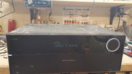
- Help with a Harman Kardon AVR3700 SMPS