.....
My goal would be have a high slew rate capability of course with such a high LTP Iq...
You are not using Miller compensation so the LTP current is not the current going in and out of the compensation cap, hence NOT deciding the slew rate. In the schematic in post #266 the compensation caps are charged and discharged by the feedback resistors of very low impedance (slightly smaller than 47-R), that was why you had a gigantic slew rate in simulation.
BTW - if that's already the case - do you have any other suggetions?
Should I change some of my BJT types for example?
Smaller ß in the LTP..? Other types for the CCS..?
About LTP quiescent currents: in itself why it is a problem even it'd be ~10mA?
Except the dissipation what other effect/disadvantage it has?
(My goal would be have a high slew rate capability of course with such a high LTP Iq...)
Well, in general, I have already outlined most of my recommendations, related to your design
")
LTP quiescent current - it can be higher, no problem, although this is not going to help too much in this kind of topology, assuming you will use Miller compensation, which is a normal practice for this kind of VFA design. The drawback may be the higher noise from the input stage. Talking about reducing the quiescent current, I mostly meant the drivers/pre-drivers. Those are rather stressed and this is one of the factors, decreasing stability. All the other quiescent currents, shown in post #255, are selected according to reasonable impedance matching and power dissipation considerations.
If you want to go for some really high slew rates, you should go for CFA topology - here is a couple of examples from my own "library"
:CF-FET V2.0
VERTICAL CFA
BTW - if that's already the case - do you have any other suggetions?
Should I change some of my BJT types for example?
Smaller ß in the LTP..? Other types for the CCS..?
About LTP quiescent currents: in itself why it is a problem even it'd be ~10mA?
Except the dissipation what other effect/disadvantage it has?
(My goal would be have a high slew rate capability of course with such a high LTP Iq...)
Voltage gain is Av=gm (milli-Siemens) times the load in k.Ohms
gm is temperature related and it is equal to the current in m.a. divided either by 26 m.V. or 25 m.v. - so you have either 38.46 m.S. per m.a. or 40 m.S. per m.a. of collector current.
The load is the value of the collector in parallel with the input resistance of any following stage. With a common collector amplifier it will be low RIN (k.Ohm) = Beta/(Ic in m.a./26 m.V.) 25 m.V. might be used instead of 26 m.V. the difference is not that significant.
The RIN of an emitter follower stage ( your output triple) will be higher on the other hand. These have a voltage gain of a little less than one.
It follows from this that if voltage gain is to be reduced to one at some frequency in advance of where the feedback phase angle reaches -180 degrees this has to be done around the Vas.
The emitter follower stages are for current gain. In terms of voltage the gain is a little less than one which is as low as it needs to be to start with.
The first thing to get right is the dominant compensation around the Vas stage. With three 3.9 pF capacitors totally 12 pF you simply don't have enough to do the job.
After sorting that you might need some phase correction in the signal stages of the amplifier. Phase correction networks might be needed in high loop gain amplifiers, there are none in the amplifier you used for your model.
You would have more certainty in your direction if you reverted your resistor values to match the model as this has a popular following on this site.
Hi Cortez, before you dive into another layout design maybe you want to give the existing boards a last ditch attempt.
Your schematic with post #266 is employing Miller Input Compensation (my last post saying you were not using Miller compensation was not entirely precise. I meant to say you were not using Conventional Miller Compensation, in which the compensation cap stays local to the VAS), yet you have an overly aggressive gain crossover frequency far out at 3.29MHz, which likely is the cause of the instability. The schematic with post #225 had it at stunning 6.18MHz and that would surprise everyone had it not oscillated.
This gain x-over frequency in such a compensation setup is derived from C3+C4 and R22, that's 22pF and 2K2 with post #266 circuit. Usually a gain crossover frequency of 500KHz is a good starting point to design an amp, and 1MHz probably is considered to be mildly aggressive. With C3=C4=11pF, you may want to increase R22 to 15K to bring the Fgxo down to 482KHz. R21 could be increased to around 470R-680R to maintain a reasonable closed loop gain.
If possible, insert a 1K5 resister to go in series with C3 and C4. They can help the phase at higher frequencies.
Get rid of C9 and C10 for now, as "you don't want to fight them all at once" -- Valery
If it's still found unstable, R29-C13 network shown in #225 can be put in as needed, but C13 needs to be increased to 1,600pF to be hopefully effective.
That's exactly what I did this evening and maybe (just maybe..!) I have some hope...before you dive into another layout design maybe you want to give the existing boards a last ditch attempt
In the morning I repaired my half-way-smoked IPS and googled this compensation topic.
I found TPC and gave it a try...
I started in reality just with the miller and the incrementally/experimentally
a lot of C values in almost every combination...
A finished with an intresting combination with just 2x10pF miller, 33pF from
VAS PD, 10pF from VAS ND and the original 47pF going to the current mirror.
The result was quite good with the standalone IPS even up to 20Vpp levels.
Then I tried with OPS but it oscillates but the modulated waveform looks
"good", so I hope maybe now it's basically just my nasty OPS...
So tomorrow I'll try to MOD it according to your suggestions:
Reducing quiescent currents and placing RCs to the pre-driver and driver stages as needed...
Results:
- #1: simulated bode: looks OK (but as you told me maybe this doesnt
mean anything due to the multiple compensation loops...)
Phase margin = 88°, Gain margin = 20dB
(Oh you cannot imagine how I wish this would be the reality as well...) - #2: simulated transient analysis shows no overshoot and a ~190V/us slew rate
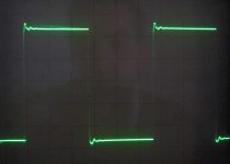
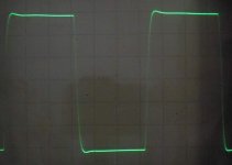
(input signal risetime = 1ns, input filter removed) - #3: scopeshot with 200kHz @ 5V/DIV and the indispensable oscillation of course...
(Sometimes it's better just when I touch the VAS to OPS PD/ND wires/solder joints...)
Schematics attached as well...
Attachments
That's exactly what I did this evening and maybe (just maybe..!) I have some hope...
In the morning I repaired my half-way-smoked IPS and googled this compensation topic.
I found TPC and gave it a try...
I started in reality just with the miller and the incrementally/experimentally
a lot of C values in almost every combination...
A finished with an intresting combination with just 2x10pF miller, 33pF from
VAS PD, 10pF from VAS ND and the original 47pF going to the current mirror.
The result was quite good with the standalone IPS even up to 20Vpp levels.
Then I tried with OPS but it oscillates but the modulated waveform looks
"good", so I hope maybe now it's basically just my nasty OPS...
So tomorrow I'll try to MOD it according to your suggestions:
Reducing quiescent currents and placing RCs to the pre-driver and driver stages as needed...
(Sometimes it's better just when I touch the VAS to OPS PD/ND wires/solder joints...)
[/LIST]
Schematics attached as well...
Get rid of the lead capacitor in parallel with your feedback resistor. This not only connects to the inverting input but also through the two other capacitors connected on either side of your Vas.
You do not want any remotely spurious signal at the output being recycled or given prominence.
Since you have a capacitor connecting the collector and emitter of your Vas you only need one off compensation capacitor - that at the collector connecting to your inverting input.
This method of compensation does not deliver as favourable distortion figures at 20 kHz as do Miller compensation schemes loved by many.
On the other hand with the right value the bypass feedback path to the inverting input has advantages if you are having problems in achieving stability. I have seen this type of compensation referred to as "feed forward" a somewhat loose description.
I have just repaired an old Kenwood KA-3500 amplifier for my brother which has a mix of "feed forward" and Miller compensation - predominantly Miller. The circuit is available at Hi-Fi Engine website. I have the circuit of an Adcom amplifier said to have been designed by Nelson Pass that uses this strategy as well. You might look at this as a possible stage 2 exercise for the future.
If you take out the lead compensation capacitor as suggested you are going to need to make an adjustment - more convenient if you have to change only one capacitor. Any trial and error approach might be helped if you insert some pcb pins into the holes where the compensation capacitor connect - so you can solder the trial capacitor in place from the top side of the board. The length of the pins should allow other values to be soldered in parallel.
You could get a quantity of 100 pF and 47 pF caps and fit two of each between the spaced pins to make roughly 390 pF. If stable then you would snip out one of the 47 pF's if not you would replace it with a 100 pF.
Last edited:
What? You tried TPC? And it oscillated? Really? Did that surprise you? I guess not. How did you come up with the component values? What was your intended gain crossover frequency? What is the next on your list and how are you going to butcher that one? your know...Mr. Béla Bartók, a great country man of yours....he did not just threw notes around and they became Bluebeard's Castle. Didn't mean to discourage but you seem to need to focus yourself and try to understand what you're doing. Get that book of Bob Cordell's. It will save your life.
your know...Mr. Béla Bartók, a great country man of yours....he did not just threw notes around and they became Bluebeard's Castle. Didn't mean to discourage but you seem to need to focus yourself and try to understand what you're doing. Get that book of Bob Cordell's. It will save your life.
Last edited:
@ Cortez,
The purpose of this forum is to share ideas and to inform.
You don't have to accept any ideas put forward, however if contributors form the impression they are wasting their time, and can see no resulting outcome they will drift away silently to threads where they can feel more involved.
The purpose of this forum is to share ideas and to inform.
You don't have to accept any ideas put forward, however if contributors form the impression they are wasting their time, and can see no resulting outcome they will drift away silently to threads where they can feel more involved.
Today I found this layout:
http://bovan.net/gmweb2/gem100.gif
(Explanation: The GEM)
And that unconventional 10n at LTP Q2 B-E.
I tried and tuned the values and it works for me...
Beyond that there are 2 comp caps:
100pF from LTP current mirror B
and 47pF from VAS PD to FB.
I modded the OPS as well:
Changed the quiescent currents according to Valery's reccomendations.
RCs there: 33p on predrivers 22R driver base stopper + 100pF CB.
And take out the 680nF || on the driver emitter resistor.
But that wasnt dominant maybe it will help with long term stability
but didnt change much on the square wave response.
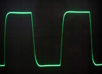
Result attached. (200kHz @ 5V/DIV, 47pF @ input)
Its stable even without input cap but then it has some overshoot and ringing.
http://bovan.net/gmweb2/gem100.gif
(Explanation: The GEM)
And that unconventional 10n at LTP Q2 B-E.
I tried and tuned the values and it works for me...
Beyond that there are 2 comp caps:
100pF from LTP current mirror B
and 47pF from VAS PD to FB.
I modded the OPS as well:
Changed the quiescent currents according to Valery's reccomendations.
RCs there: 33p on predrivers 22R driver base stopper + 100pF CB.
And take out the 680nF || on the driver emitter resistor.
But that wasnt dominant maybe it will help with long term stability
but didnt change much on the square wave response.
Result attached. (200kHz @ 5V/DIV, 47pF @ input)
Its stable even without input cap but then it has some overshoot and ringing.
Attachments
Today I found this layout:
http://bovan.net/gmweb2/gem100.gif
(Explanation: The GEM)
And that unconventional 10n at LTP Q2 B-E.
I tried and tuned the values and it works for me...
Post an imagine of your scope using a 10 kHz square wave with a load of 8R in parallel with 2uF and see if it does not come unstuck.
Guys you must explain this...
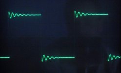
Out of curiousity I just tried a 100n(!) C there at LTP Q2 B-E and it's even better so...
Check out the results: (Sorry for the blurred images I just made them in hand...)
Out of curiousity I just tried a 100n(!) C there at LTP Q2 B-E and it's even better so...
Check out the results: (Sorry for the blurred images I just made them in hand...)
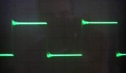
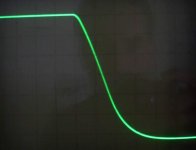
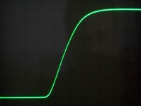
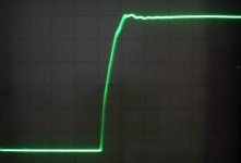
- 200kHz @5V without input filter
- positive edge
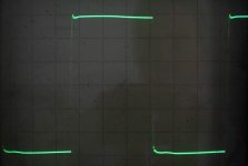
- negative edge
- capacitive load = 2u2 @ 10kHz (5V/DIV)
(though the 22R current limiters are still in...)
Attachments
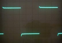
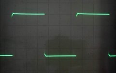
Take a better picture with 2u2 || 10R @ 10kHz 5V/DIV (current limiter reduced to 3R5/rail).
Strange that its a bit squared and not smooth and rounded sinus like...
But maybe it's due to the testing layout and long rail wires.
Even the Power ground is now taken from far from the PS center GND point.
Strange that its a bit squared and not smooth and rounded sinus like...
But maybe it's due to the testing layout and long rail wires.
Even the Power ground is now taken from far from the PS center GND point.
Attachments
Don't worry about the images in your post #293.
The diode resistance between the emitter and base of a transistor varies according to the amount of current being passed. Temperature has an effect however with paired devices the effects of each in an LTP should cancel out.
When conducting the emitter to base junction is said to be forward biased and in this state it will develop a significant amount of capacitance between these two points - more than Miller capacitance developed between the collector and base of a common emitter amplifier such as the separate elements of an LTP or a Vas.
In an LTP the separate transistors will have varying emitter diode resistance and varying emitter to base capacitance.
Miller capacitance has the effect of reducing high frequency response. Emitter to base capacitance works in opposition to the Miller capacitance but it is of no significance when the capacitance at either of these two junctions is subject to constant variation.
External emitter to base capacitance provides a constant capacitance value.
With a largish value of capacitor in that role the characteristics of that junction provide a route for a.c. signals to bypass the variables of diode resistance and junction capacitance.
The aim of this strategy in the case of Maynard's circuit seems to be to emulate the single transistor input of Linsley-Hood's Class A amplifier for a.c. signals while leaving the d.c. conditions of the LTP intact.
Linsley-Hood's Class A amplifier was a project anyone could build as it was stable without additional components to stabilise it.
He later built a version with an LTP input. A seemingly simple change that involved the compromise of having to do so.
If I remember correctly the word he used was "incipient". Linsley-Hood has published designs incorporating LTP input stages - these needed more attention to compensation and phase adjustment.
I think you have demonstrated you can get some measure of stability with this amplifier. Looking back to posts 31 and 33 on page 4, you should be able to get this sorted without having to resort to "out on a limb" methods.
So now its a simple transistor amp instead of a symasym?
And 3-4 bjts are just for DC?
I'll simulate it tomorrow.
Though its stable and performs very good.
I tested with 10uF load and then with 100kHz 4R7 load and both were perfect.
I had an idea similar what you said: it's now a CFA
as the FB skips LTP Q2 directly to Q1 emitter right?
And 3-4 bjts are just for DC?
I'll simulate it tomorrow.
Though its stable and performs very good.
I tested with 10uF load and then with 100kHz 4R7 load and both were perfect.
I had an idea similar what you said: it's now a CFA
as the FB skips LTP Q2 directly to Q1 emitter right?
So now its a simple transistor amp instead of a symasym?
And 3-4 bjts are just for DC?
I'll simulate it tomorrow.
Though its stable and performs very good.
I tested with 10uF load and then with 100kHz 4R7 load and both were perfect.
I had an idea similar what you said: it's now a CFA
as the FB skips LTP Q2 directly to Q1 emitter right?
That is the way I looked at TR1 and TR2.
I am not doing any design work and learning SPICE is not on my agenda. All I can give is some thoughts you might care to investigate with your software.
I cannot see the 100n bypass capacitor acts to reduce loop gain at high frequency. On that basis it would not replace the need for Vas compensation.
The signal from Vas needs to arrive at TR1 emitter - as outlined previously the LTP operates in push pull and base currents and junction capacitance between base and collector and emitter and base will fluctuate accordingly.
How significant or whether significant at all I don't know, however bypassing TR2 has had some effect on stability.
A compensation capacitor of 4p7 will pass a very tiny amount of a.c. current and how does this progress through TR2 emitter to base diode under push-pull operating conditions. A larger compensation capacitor would pass more current and have greater headway - I suggested a value of 390 pF for starters.
As to TR2 emitter to base capacitor bypass in combination with 4.7 pF maybe the capacitor path is cleaner and this changes the dynamics.
LTP stages generate half the voltage gain of a single input device. Bypassing TR2 emitter to base with a capacitor will work against voltage gain reduction for a.c. signals and this could be important at high frequency.
I have not kept up with the pace of your changes so there may be some point I have missed. I would be good to see an update of your circuit.
I simulated the amp with this 100n and it looks like still both tails are working in AC as well both at LTP and VAS.
I attached the latest schematic both in open and closed loop analysis modes.
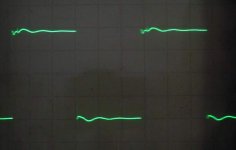
And some pictures as well, in order:
I attached the latest schematic both in open and closed loop analysis modes.
And some pictures as well, in order:
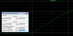
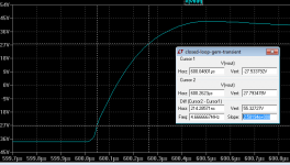
- spice transient shows a little overshoot without input cap
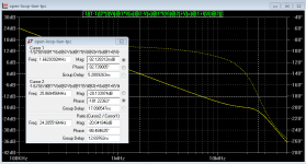
- slew rate in theory is 260V/us
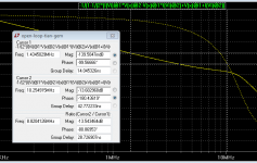
- tian bode: phase margin = 80° gain margin = 13.7dB
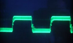
- my function generator isnt ideal at all... (100kHz)
- the same with different voltage level
- rising edge (still just my generator)
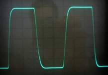
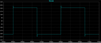
- amplifier doing 100kHz @ 5V/DIV on a 4R7 dummy load
- testing with 10uF capacitive load @ 10kHz 5V/DIV (no current limiters now)
Attachments
-
open-loop-tian-gem.asc16.4 KB · Views: 26
-
 8-10u-5v-div.JPG36.8 KB · Views: 37
 -
 7-100kHz-4r7.JPG39.9 KB · Views: 38
 -
 6-fn-gen-3.JPG38.1 KB · Views: 33
 -
 5-fn-gen-2.JPG39.2 KB · Views: 29
 -
 4-fn-gen-1.JPG38.6 KB · Views: 36
 -
 3-lt-bode.PNG29.6 KB · Views: 30
 -
 2-lt-slew.PNG24.2 KB · Views: 29
 -
 1-lt-transient.PNG21.3 KB · Views: 34
 -
closed-loop-gem-transient.asc15.2 KB · Views: 27
Oh, I almost forgot to tell: the OPS mod was necessary!
Yesterday I tried to remove/decrease the Ccb caps @ driver stage but then it started to oscillate!
With the 22R base stoppers at the drivers base 100pF was a good value.
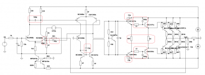
Made a schematic and marked the mods made compared to the original design.
Yesterday I tried to remove/decrease the Ccb caps @ driver stage but then it started to oscillate!
With the 22R base stoppers at the drivers base 100pF was a good value.
Made a schematic and marked the mods made compared to the original design.
Attachments
Check the quiescent current (bias) of the output stage with the NFB and Output Zobel connected. But disconnect the load.
The sum of the three currents of the upper half should equal the sum of the three lower half currents. And short the input.
If you have matched outputs very well you may end up with a spread of <5% between the highest and lowest of the three.
But more likely you will see a spread of 10% to 20%
Unfortunately shorting the input of a DC coupled amplifier upsets the output offset. If you had a load connected, then that output offset could account for unbalance of the upper and lower currents.
Last edited:
- Status
- This old topic is closed. If you want to reopen this topic, contact a moderator using the "Report Post" button.
- Home
- Amplifiers
- Solid State
- Heatsink vs OS stability