I think matching by measuring individuals is worthless for us amateurs who cannot control Tj.Ho much matching do you think is necessary for this frontend? I just measured 10 Fairchild BC550C's. They ere mostly ithin .3mV of each other, but never larger than .8mV apart. In the simulator I find a 2.7mV mismatch causes a 10% current difference in an LTP and a .3mV difference causes a 1.1% current difference.
I repeatedly recommend REF&DUT matching to make some attempt at holding similar Tj between DUT and REF.
If Tj is uncontrolled then one cannot possibly rely on any measurements.
Ref your 0.3mV or sim at 2.7mV This would almost certainly have been revealed had you clamped the two devices together and applied the Test & Measurement jig to the pair. Matching of the collector currents to <1% is not easy. Most importantly the resistors must be selected to be <<1%. The base resistors must also be allowed for, or shorted out, otherwise a small difference in hFE will draw different base currents and the base resistor then applies a Vbe diff due to the different Base resistor Vdrop.
By the Way, I don't match Vbe. I send the same voltage to both bases. I measure the absolute collector currents and the differential collector voltages. If the REF & DUT has a small Vbe mismatch then the jig throws this out as a severe Ic mismatch. Try the next pair.
I swing the test Ic either side of operating bias current by adjusting the applied base voltage. If the REF & DUT track (near zero differential collector voltage) over a decent range of Ic, then I have a matched pair.
Last edited:
Don't include me in that company. I only read, assess, choose/bin and then test. I don't "design" anything. I copy what I think are the "good enough" proposals and try to implement in a useful way.I already satisfy Self, Cordell and ..............and now Edmond will like it too
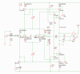
Ah, ok. What I see in that post is what I meant by a diamond buffer + EF triple (as what I mean is [diamond buffer + EF] triple, rather than [diamond buffer] + [EF triple]). Arthur, where did your transistor models come from? Many are really poor. If the models for the drivers aren't great, how about trying my 2SC5171/2SA1930 models? And for the final output devices, I wonder if using 1302/3281 output transistors would make much difference as these have flatter beta vs. Ic, and higher Vceo with possibly correspondingly lower early effect (although this doesn't always go hand-in-hand).
Hello Harry,
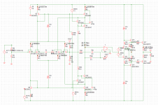
My previous sims where with Fairchild models predrivers KSC2690 and KSA1220, and Sanken supplied models of the 2SA1216 and 2SC2922, all other models are Cordell derived types.
Thank you for your work on the 2SC5171/2SA1930 models attached are some sims using them with (Cordell models) MJL1302C/MJL1302C. I also included simulations showing an additional ideal buffer between the TIS input stage and diamond EF output stage which provides perfect loading of the TIS stage and I think the results speak for themselves.
Arthur
Attachments
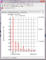
Thanks for your efforts Arthur; most intriguing! Looks like different transistors make near-as-damn-it no difference, and the addition of an ideal buffer also makes no difference. Presumably this means the triple isn't upsetting the performance of the front-end but we're merely seeing a limit on the performance of this type of output stage? If this is the case I'm surprised that this is nearly 0.003%; I would have expected somewhere between 1 and 10 ppm (although I haven't seen a loop-gain plot so is loop gain from 20 - 100 kHz just not that high?). What happens if you add a second pair of output devices?
Could you also probe the output of the front end (i.e. the node joining Q8 and Q12 collectors) and calculate distortion at this point?
Could you also probe the output of the front end (i.e. the node joining Q8 and Q12 collectors) and calculate distortion at this point?
Hello Harry,
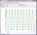
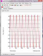
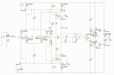
See attached schematic and THD plot.
Regards
Arthur
oops! I wasn't thinking was I? To linearise the output stage, a pre-distorted signal must be applied at its input. So when negative feedback is working, we would expect the front end to have a distorted output!
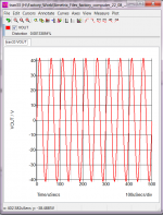
THD with 2 pairs.
Hello Harry,
Even when I load the TIS_VOUT node with 100k it has very little effect on the THD at the output across the 8R load.
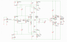
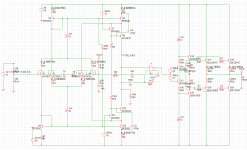
Attached is the THD simulation with 2 output pairs.
Regards
Arthur
Hello Harry,
Even when I load the TIS_VOUT node with 100k it has very little effect on the THD at the output across the 8R load.
Attached is the THD simulation with 2 output pairs.
Regards
Arthur
Attachments
oops! I wasn't thinking was I?
I had to rethink too.
To see the distortion of the superTIS we need to take the feedback from the superTIS output.
Will need to be buffered but that is easy, can we see that, Arthur?
Best wishes
David
PS
Pheonix said:Even when I load the TIS_VOUT node with 100k it has very little effect on the THD at the output
Perhaps my concern about the load on the superTIS has been based on a faulty assumption all the time.
Last edited:
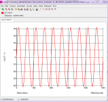
TIS THD with ideal ouput stage
Hello Dave and Harry,
The TIS stage by itself has very low THD its fair to say that the main source of distortion is the conventional diamond EF output stage. Even the simulation with the addition of the ideal buffer between the TIS output and conventional output made a very small difference and I don't think its worth the effort.
Regards
Arthur
Attachments
Hello Guys,
What I find interesting is how linear the stage actually is with the Baxandall super pair. I too thought that the reason the Baxandall folded cascode worked so well was because it had such high output impedence and hence high gain, but the Baxandall super pair makes a very linear transistor stage by (to quote Edmond) removing nonlinear impedances: Cob and Early effect.
By simulating I think it is fair to say that you need an error corrected output stage to get the best out of the TIS input stage.
Arthur
Thanks
Thank you for those simulations and to Harry for resurrection of the issue. Very instructive about the role of the OPS.
I now feel closer to finalization of my amp.
Any comments from you or Harry about my rationale for a CFP + EF OPS?
Best wishes
David
Crossed posts. Rather than error correction I plan to reduce the distortion with some simple brute force!
Lots of fast output transistors and low emitter resistors with plenty of bias for the EF.
And the class A-ish CFP pre-driver & driver.
Yes it will run warm. Canberra is usually cool and often cold so I don't care!
The TIS stage by itself has very low THD its fair to say that the main source of distortion is the conventional diamond EF output stage. Even the simulation with the addition of the ideal buffer between the TIS output and conventional output made a very small difference and I don't think its worth the effort.
Thank you for those simulations and to Harry for resurrection of the issue. Very instructive about the role of the OPS.
I now feel closer to finalization of my amp.
Any comments from you or Harry about my rationale for a CFP + EF OPS?
Best wishes
David
Crossed posts. Rather than error correction I plan to reduce the distortion with some simple brute force!
Lots of fast output transistors and low emitter resistors with plenty of bias for the EF.
And the class A-ish CFP pre-driver & driver.
Yes it will run warm. Canberra is usually cool and often cold so I don't care!
Last edited:
slow CFP
Hi David,
Harry probably meant by 'slow' the long turnoff time of a CFP BJT OPS. This is because the output trannies are turned off only passively (by means of resistor between base and emitter), instead of actively (by means of a driver).
BTW, I don't like CFPs either.
Of course you can use TMC. What Self said about it is irrelevant, as he even doesn't know to implement TMC correctly (wrong capacitor ratio).
Cheers,
E.
.............
You say "they are slow". Not sure I follow.
Hi David,
Harry probably meant by 'slow' the long turnoff time of a CFP BJT OPS. This is because the output trannies are turned off only passively (by means of resistor between base and emitter), instead of actively (by means of a driver).
BTW, I don't like CFPs either.
Can we use TMC in a CFP? I already satisfy Self, Cordell and AndrewT and now Edmond will like it too
Best wishes
David
Of course you can use TMC. What Self said about it is irrelevant, as he even doesn't know to implement TMC correctly (wrong capacitor ratio).
Cheers,
E.
Harry probably meant by 'slow' the long turnoff time of a CFP BJT OPS. This is because the output trannies are turned off only passively (by means of resistor between base and emitter), instead of actively (by means of a driver).
Yes, but I already clarified that my plan is NOT CFP output transistors.
It is the use of a CFP [pre-driver + driver] to drive an EF output.
As opposed to 2 cascaded EFs to drive the EF output.
Adequate bias means that effectively the CFP is class A so I don't see a problem.
Except potential local oscillation. You know any helpful analyses of the optimal way to prevent this?
I like to consider a CFP as a little feedback loop so intuitively it seems reasonable to use the same tools that work well globally.
So I meant to use TMC within the CFP loop. Not just an amplifier with overall TMC compensation and a CFP in the OPS.
I hope this is clear.
Best wishes
David
Last edited:
Dave, do you mean an OPS as in this amp?http://www.diyaudio.com/forums/soli...-stage-audio-power-amplifier.html#post1349109
Damir
Damir
I think matching by measuring individuals is worthless for us amateurs who cannot control Tj.
I repeatedly recommend REF&DUT matching to make some attempt at holding similar Tj between DUT and REF.
If Tj is uncontrolled then one cannot possibly rely on any measurements.
Ref your 0.3mV or sim at 2.7mV This would almost certainly have been revealed had you clamped the two devices together and applied the Test & Measurement jig to the pair. Matching of the collector currents to <1% is not easy. Most importantly the resistors must be selected to be <<1%. The base resistors must also be allowed for, or shorted out, otherwise a small difference in hFE will draw different base currents and the base resistor then applies a Vbe diff due to the different Base resistor Vdrop.
By the Way, I don't match Vbe. I send the same voltage to both bases. I measure the absolute collector currents and the differential collector voltages. If the REF & DUT has a small Vbe mismatch then the jig throws this out as a severe Ic mismatch. Try the next pair.
I swing the test Ic either side of operating bias current by adjusting the applied base voltage. If the REF & DUT track (near zero differential collector voltage) over a decent range of Ic, then I have a matched pair.
Andre, your logic matches mine. All transistors ere snug up against each other in a line on my breadboard. I used the resistance function on my DMM to measure Vbe since I kno it's test current is 200uA. I did it this ay because there ould be no resistor or PSU tolrance/drift to orry about. I measured Vbe's 3 times and the measurements drifted a bit but ere consistent. This as just an experiment to get an idea hat the spread of values could be. It is nice to kno that, most of the time I could pick up to Fairchild BC560C's and they ould be Vbe matched ithin 5%, for current mirror purposes. I doubt that temperature variances ould selectively alter Vbe to bring the transistors closer.
The importance of Hfe matching depends a lot on the circuit. For an LTP, Hfe matching is only really useful if you need lo offset or if the input and feedback impedances are matched at the frequencies in question.
PS: You'd be surprised ho many programs ill crash if you just have a mouse that doubleclicks itself.
Dave, do you mean an OPS as in this amp?http://www.diyaudio.com/forums/soli...-stage-audio-power-amplifier.html#post1349109
Damir
Yes, similar except for any improvements I can make. MJL4302 and MJL4281 outputs that are a bit faster. Probably Thermal Trak diodes in series with a smaller R5 and Vbe transistors bolted to Q19 and Q20 for ambient temperature compensation in addition to Thermal Trak diodes, all very similar to your amp.
")
Best wishes
David
Kean, you are missing the vital difference.
The transistors operate in the circuit as voltage to current converters.
Apply a Vbe and the output is a current.
A 5% difference in applied Vbe is enormous. The output current change will be enormous. That is not the same as testing for hFE.
If you want to see if two transistors match for LTP or mirror or similar where the two devices use applied Vbe to generate an output current then you must test them as a balanced pair. Look at Anatech's jig, I think Cordell proposed a similar jig. Recently Fritz (or something like that) showed a balance jig.
You really must apply the same Vbe to each, simultaneously, while the devices are Thermally Coupled to get reasonable matching results.
Hi David,
You will need at least a triplet. Don't forget that the super TIS has one gain stage less than a conventional front end. So you need a pre-driver to compensate for the lack of (current) gain anyhow. But even with a conventional front end, a triplet is recommended. That means that using the super TIS instead, you will probably need a quartet. (Oh, and don't forget to bootstrap the collectors of the pre-driver)
Now the question raises has anyone built a quartet OPS and how difficult it is to tame such an OPS?
Cheers,
E.
The only quartet I could get to work well without stability issues is using a diamond buffer driving a driver, driving output transistors, very much the same as you have shown on your webpage. I got the idea from pioneer that used this setup in early 1990s as outputstage in their top of range amp lineup. If youd like I can send you schematics although your outputstage is very much the same. The usual miller cap on the drivers and base resistors on the outputs are enough for stability.
- Status
- This old topic is closed. If you want to reopen this topic, contact a moderator using the "Report Post" button.
- Home
- Amplifiers
- Solid State
- Has anyone seen this front-end before?