I've been intrigued by the Hall notch filter posted recently
http://www.diyaudio.com/forums/equi...-tune-my-twin-t-notch-filter.html#post4895451
Rediscover The Truly Tunable Hall Network | Analog content from Electronic Design
and had to give it a try! Here are some results that might be interesting to anyone else messing with this filter.
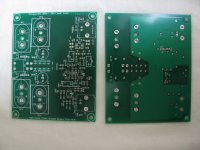
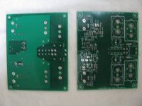
I've had 3 test PC boards fabricated. All 3 are an exact copy of figure 7 in the EDN article link above. An input unity gain buffer, and output unity gain buffer, and yet another unity gain buffer fed by a pot as resistive divider on the output for positive feedback level. The difference between the boards is in op-amp type. There is a "single output chip" board that uses two individual single op amps for the two output unity gain buffers. Then there is a "dual output chip" board which uses one dual op-amp for the two output buffers. Then on all 3 I also have an output gain stage, but for now I have it unpopulated and bypassed with that white wire. The Hall filter as implemented is unity gain. Then there is a third board that is exactly the same as the single output chips, just without the notch out in the ground plane. Just curious if it makes a difference.
The reason for the two board types is that I could get the Hall to simulate (LT Spice) beautifully with OPA827's, which are only available as single, but my real intent was to use anOPA1641 for input buffer and OPA1642 for the output buffers. But the LT Spice sim would just lock right up with the OPA16xx. Tried setting initial condition voltages and several other things. No luck. So... figured I would cover all bases and maybe one of the two board types would work, especially since the fab house offers combined shipping.") Luckily the OPA16xx seem to work just fine in real life here. I'm going to build up boards with OPA1611's and OPA827's to see if there is any significant difference in notch depth.
Luckily the OPA16xx seem to work just fine in real life here. I'm going to build up boards with OPA1611's and OPA827's to see if there is any significant difference in notch depth.
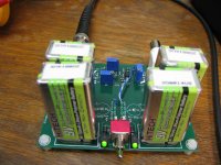
I usually do 4 layer board with two of the layers as power and one as ground, but cwtim01 made a fantastic 2 layer version of the Fliege recently in the Fliege thread, so I was motivated to give that a try! 2 layer is boatloads cheaper. The board has two 9V in series for each rail, but in the photo here I have shorting snaps over one battery on each rail. Note that two 9V primary cells would be too much, +/-18.4v or so when the batteries are fresh (chip max is +/-18Vdc). Hence the shorting snaps to allow using just one 9V for each rail. But I have the two since I've gone to these rechargeable lithium polymer recently (0.3 ohm internal resistance and 600mAhr!), 7.4V nominal and 8.4V fully charged, so no higher than +/-16.8V, just fine for the chips's +/-18Vdc maximum. These are lithium cells in the photo, I just couldn't figure out where I put the other two batteries at the moment! Around here somewhere. So this is running on +/-7.4Vdc.
Then the battery section just cables out to each chip with twisted pair, CAT5 strands in this case. The boards are sized to fit a metal box enclosures B2-080 or B3-080 case, so at some point I'll try boxing them up and feeding the power in externally. Should get rid of some noise in the output.
Results
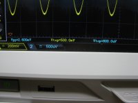
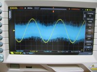
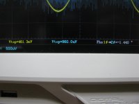
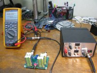
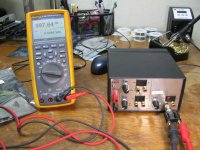
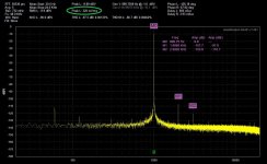
This one is a single output chip board with OPA1641's used in all 3 positions (again, figure 7 in the EDN article, watch out for the typo C1 is 6.8nF not 68nF). The schematic below has the part values, same as the EDN article, and actual part numbers. I'm feeding it with a Victor 1KHz oscillator set for 500mV peak, as can be see from the scope shots below (Vtop and Vpp at the bottom of the screen). The oscillator is on channel 1 (yellow) which is set for 200mV/div.
The hall notch filter output is on channel 2 (blue) set for 500uV/div, hence that noise envelope around the notch signal. All 3 trimmers were set to the middle with an ohmmeter before installing. As per the EDN article I adjusted the frequency trimmer first for minimum notch, R5 on my board, THEN adjusted the notch depth trimmer. Worked pretty well! Only had to do about 1/2 turn of either from the ohmic pot center. Then I tried the posititive feedback trimmer, R12, which didn't have much of an effect on anything. I was impressed that the signal didn't move out of the notch over time! The Victor Oscillator drifts a few Hz over time (probably thermal) and I've had it drift right out of other narrow notch filters (my Fliege). The notch bottom on this thing is pretty wide.
With the notch adjusted for minimum it appears to me that the signal part is around 750uV peak, and the scope seems to agree at the bottom (Vtop), even though the total noise envelope is about twice that. On this lowest 500uV/div range the scope's vertical amplifier itself is noisy too, about 0.2mV worth. Running with the 750mV peak figure gives 0.75mV/500mV = -56dB! Works for me. Now if using the metal case would just get rid of some of that output noise (fluorescent lights on in here right now) it would be even better.
Photos:
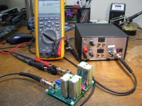
* 4675 is the single output chip board, 69 is the test setup. Those are Victor Oscillators in the box on the right.
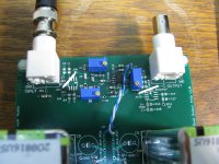
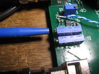
* 70, 71, and 72 are the single output chip Hall notch board, taken right from figure 7 in the EDN article linked above, using all OPA1641 chips. The 4th chip, an output voltage gain stage, is unpopulated and bypassed with the white wire. The empty JP holes are just test points. I put in a ton of them! test points on the input and output of every op-amp. Turned out to be quite useful. On first power up I was getting the full 7Vdc rail voltage injected into the passive notch filter parts somehow. Tracked it down to a bad solder connection on one pin of IC3, the positive feedback op amp.
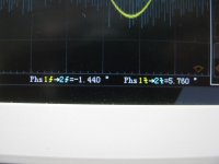
* 73 and 74 are scope shots. Yellow is the input from the Victor 1KHz oscillator, blue is the notch output from the Hall notch filter with the trimpots adjusted for minimum notch. Best I can tell (and also the scope's conclusion at the bottom) the signal peak is about 750uV out of the total 1.5mV peak noise envelope.
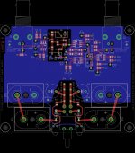
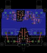
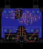
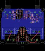
* layout and schematic (PDF) of the single output chip board. The SMD are all 0805. The four resistors under the PC board are unpopulated placeholders that would allow the two trimpots to be unsoldered, measured, then replaced with these fixed resistors.
I had a couple of regrets after the board when out to fab. I should have put a placeholder in for an output (50 ohm) series resistor. I got lucky here and no problem with BNC cable capacitance apparently (no oscillations that I could see on the scope), but that 50R might be needed with other chips. Then it would probably be wise to set that positive feedback stage up with placeholders for parts to adjust the phase. The article noted the actual measured Hall notch depth, while good, wasn't as good as the math and he suspected lead or lag phase shift in those output op-amps as the culprit. That would be an interesting experiment.
Hovering over the photos will bring up the picture number, clicking on the lower right arrows will enlarge them.
http://www.diyaudio.com/forums/equi...-tune-my-twin-t-notch-filter.html#post4895451
Rediscover The Truly Tunable Hall Network | Analog content from Electronic Design
and had to give it a try! Here are some results that might be interesting to anyone else messing with this filter.
I've had 3 test PC boards fabricated. All 3 are an exact copy of figure 7 in the EDN article link above. An input unity gain buffer, and output unity gain buffer, and yet another unity gain buffer fed by a pot as resistive divider on the output for positive feedback level. The difference between the boards is in op-amp type. There is a "single output chip" board that uses two individual single op amps for the two output unity gain buffers. Then there is a "dual output chip" board which uses one dual op-amp for the two output buffers. Then on all 3 I also have an output gain stage, but for now I have it unpopulated and bypassed with that white wire. The Hall filter as implemented is unity gain. Then there is a third board that is exactly the same as the single output chips, just without the notch out in the ground plane. Just curious if it makes a difference.
The reason for the two board types is that I could get the Hall to simulate (LT Spice) beautifully with OPA827's, which are only available as single, but my real intent was to use anOPA1641 for input buffer and OPA1642 for the output buffers. But the LT Spice sim would just lock right up with the OPA16xx. Tried setting initial condition voltages and several other things. No luck. So... figured I would cover all bases and maybe one of the two board types would work, especially since the fab house offers combined shipping.
Luckily the OPA16xx seem to work just fine in real life here. I'm going to build up boards with OPA1611's and OPA827's to see if there is any significant difference in notch depth.I usually do 4 layer board with two of the layers as power and one as ground, but cwtim01 made a fantastic 2 layer version of the Fliege recently in the Fliege thread, so I was motivated to give that a try! 2 layer is boatloads cheaper. The board has two 9V in series for each rail, but in the photo here I have shorting snaps over one battery on each rail. Note that two 9V primary cells would be too much, +/-18.4v or so when the batteries are fresh (chip max is +/-18Vdc). Hence the shorting snaps to allow using just one 9V for each rail. But I have the two since I've gone to these rechargeable lithium polymer recently (0.3 ohm internal resistance and 600mAhr!), 7.4V nominal and 8.4V fully charged, so no higher than +/-16.8V, just fine for the chips's +/-18Vdc maximum. These are lithium cells in the photo, I just couldn't figure out where I put the other two batteries at the moment! Around here somewhere. So this is running on +/-7.4Vdc.
Then the battery section just cables out to each chip with twisted pair, CAT5 strands in this case. The boards are sized to fit a metal box enclosures B2-080 or B3-080 case, so at some point I'll try boxing them up and feeding the power in externally. Should get rid of some noise in the output.
Results
This one is a single output chip board with OPA1641's used in all 3 positions (again, figure 7 in the EDN article, watch out for the typo C1 is 6.8nF not 68nF). The schematic below has the part values, same as the EDN article, and actual part numbers. I'm feeding it with a Victor 1KHz oscillator set for 500mV peak, as can be see from the scope shots below (Vtop and Vpp at the bottom of the screen). The oscillator is on channel 1 (yellow) which is set for 200mV/div.
The hall notch filter output is on channel 2 (blue) set for 500uV/div, hence that noise envelope around the notch signal. All 3 trimmers were set to the middle with an ohmmeter before installing. As per the EDN article I adjusted the frequency trimmer first for minimum notch, R5 on my board, THEN adjusted the notch depth trimmer. Worked pretty well! Only had to do about 1/2 turn of either from the ohmic pot center. Then I tried the posititive feedback trimmer, R12, which didn't have much of an effect on anything. I was impressed that the signal didn't move out of the notch over time! The Victor Oscillator drifts a few Hz over time (probably thermal) and I've had it drift right out of other narrow notch filters (my Fliege). The notch bottom on this thing is pretty wide.
With the notch adjusted for minimum it appears to me that the signal part is around 750uV peak, and the scope seems to agree at the bottom (Vtop), even though the total noise envelope is about twice that. On this lowest 500uV/div range the scope's vertical amplifier itself is noisy too, about 0.2mV worth. Running with the 750mV peak figure gives 0.75mV/500mV = -56dB! Works for me.
Now if using the metal case would just get rid of some of that output noise (fluorescent lights on in here right now) it would be even better. Photos:
* 4675 is the single output chip board, 69 is the test setup. Those are Victor Oscillators in the box on the right.
* 70, 71, and 72 are the single output chip Hall notch board, taken right from figure 7 in the EDN article linked above, using all OPA1641 chips. The 4th chip, an output voltage gain stage, is unpopulated and bypassed with the white wire. The empty JP holes are just test points. I put in a ton of them! test points on the input and output of every op-amp. Turned out to be quite useful. On first power up I was getting the full 7Vdc rail voltage injected into the passive notch filter parts somehow. Tracked it down to a bad solder connection on one pin of IC3, the positive feedback op amp.
* 73 and 74 are scope shots. Yellow is the input from the Victor 1KHz oscillator, blue is the notch output from the Hall notch filter with the trimpots adjusted for minimum notch. Best I can tell (and also the scope's conclusion at the bottom) the signal peak is about 750uV out of the total 1.5mV peak noise envelope.
* layout and schematic (PDF) of the single output chip board. The SMD are all 0805. The four resistors under the PC board are unpopulated placeholders that would allow the two trimpots to be unsoldered, measured, then replaced with these fixed resistors.
I had a couple of regrets after the board when out to fab. I should have put a placeholder in for an output (50 ohm) series resistor. I got lucky here and no problem with BNC cable capacitance apparently (no oscillations that I could see on the scope), but that 50R might be needed with other chips. Then it would probably be wise to set that positive feedback stage up with placeholders for parts to adjust the phase. The article noted the actual measured Hall notch depth, while good, wasn't as good as the math and he suspected lead or lag phase shift in those output op-amps as the culprit. That would be an interesting experiment.
Hovering over the photos will bring up the picture number, clicking on the lower right arrows will enlarge them.
Attachments
-
 IMG_4675.JPG474.1 KB · Views: 407
 -
single output chips schematic.pdf32.9 KB · Views: 114
-
 single output chips layout.jpg557.2 KB · Views: 109
 -
 IMG_4674.JPG377.4 KB · Views: 116
 -
 IMG_4673.JPG478.9 KB · Views: 129
 -
 IMG_4672.JPG598.9 KB · Views: 364
 -
 IMG_4671.JPG585.2 KB · Views: 372
 -
 IMG_4670.JPG570.2 KB · Views: 380
 -
 IMG_4669.JPG661.1 KB · Views: 379
 -
 IMG_4684.JPG454.7 KB · Views: 109
Last edited:
Nice work. You need a low pass filter on the output to get any sense of how deep the real notch is. Most distortion analyzers have 30 KHz and 80 KHz low pass filters. Or some type of swept analyzer. The output should have the harmonics of the source (below -140 dB in the Victor oscillators). I don't know if the Rigol has a spectrum function that would work for looking that deep.
One other trick I have used for devices like this is a floating supply. Two resistors and caps define the center point and then you can use 1, 2 or 3 batteries with a single switch to disconnect them. Since there should be no DC on the circuit you don't need to support much DC current through ground. 2 10K resistors to define the ground should work fine. For gadgets like this it makes things much simpler. I have a number of boxes done this way.
For measuring distortion the input opamp may limit the ultimate performance. However getting 40 dB of notch depth and 40 dB of gain at the output would "amplify" a distortion analyzers lower limit by 40 dB (or take -100 dB and make it -140 dB, essentially SOTA).
I may explore building one for a filter function for my Boonton. Only useable at a single frequency, but still a need addition.
Or some type of swept analyzer. The output should have the harmonics of the source (below -140 dB in the Victor oscillators). I don't know if the Rigol has a spectrum function that would work for looking that deep.
This is/was some special interests on my FFR (Fast Freq. Response Test Bench). While freq. stepping requires a long run specially as AP using small freq. steps.
Samuel was helping out to do such stepping tests on AP's notch to get into the knee of the notch.
A fast alternate would be white noise and afterwords use spectrum averaging.
My FFR allows up to freq. steps of sample rate / 256k in one single processing. May look at RME's ADI-2 Pro handbook
Hp
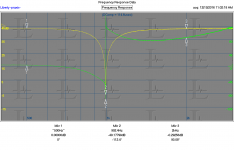
I thought I would try my speaker measurement system to see if it can plot the notch correctly. This is a plot using Praxis at 192/24 using a 500 mS chirp and a 262K FFT. I use a Kaiser 7 window. It seems to work well for a frequency response test with accuracy and high resolution. The plotted notch depth matches what I measured manually. Lots quicker than stepping an AP through a range of frequencies. This system also plots the phase response.
The DUT is a twin T notch with a shunt resistor I'll be setting for -40 dB to match the output gain. This uses my battery supply trick.
The DUT is a twin T notch with a shunt resistor I'll be setting for -40 dB to match the output gain. This uses my battery supply trick.
Attachments
One other trick I have used for devices like this is a floating supply.
Thanks for sharing! I'll keep that trick in mind.
I agree on the input op-amp, I have it set up where than can be left unpopulated and bypassed. In the sim that did work, with the OPA827's, the circuit seemed to not care too much about source impedance given the relatively large resistor values involved. All that input op-amp is likely doing is adding some noise.
I'm wondering if setting the positive feedback buffer op-amp, IC3, up as an all-pass filter would be a good way to make a variable phase shifter
https://en.wikipedia.org/wiki/All-pass_filter
https://labcit.ligo.caltech.edu/~vsanni/ph5/pdf/BasicOpAmpApplications.pdf (opens PDF, section 5.8)
A plus is swapping the pot and cap in the second link switches from lag to lead. A PCB could probably be set up to allow either configuration. Any thoughts on it out there? I do think the EDN author is right, any phase shift in the output and positive feedback op-amps is probably costing some notch depth. But how to do it so as not to turn the thing into an oscillator at frequencies away from the notch.
https://en.wikipedia.org/wiki/All-pass_filter
https://labcit.ligo.caltech.edu/~vsanni/ph5/pdf/BasicOpAmpApplications.pdf (opens PDF, section 5.8)
A plus is swapping the pot and cap in the second link switches from lag to lead. A PCB could probably be set up to allow either configuration. Any thoughts on it out there?
I do think the EDN author is right, any phase shift in the output and positive feedback op-amps is probably costing some notch depth. But how to do it so as not to turn the thing into an oscillator at frequencies away from the notch.
Last edited:
It seems to work well for a frequency response test with accuracy and high resolution. The plotted notch depth matches what I measured manually.
The question arises for me: If you zoom into the knee of the notch, do you get equal -40 dB or do you will get a higher value
While it's the question of the underlying spectrum detector. While your Data to Pixel (linear calculated) ratio is about 2.6.
Hp
The question arises for me: If you zoom into the knee of the notch, do you get equal -40 dB or do you will get a higher value
While it's the question of the underlying spectrum detector. While your Data to Pixel (linear calculated) ratio is about 2.6.
Hp
I'll find out! I haven't had a chance to try the low pass filter trick yet. That should help.
I have test points at the input to IC2 and output of IC3. I should be able to just measure on the scope how much shift exists using the OPA1641s. I probably should verify there is a problem before I try to solve it!
The question arises for me: If you zoom into the knee of the notch, do you get equal -40 dB or do you will get a higher value
While it's the question of the underlying spectrum detector. While your Data to Pixel (linear calculated) ratio is about 2.6.
Hp
I think I understand what you are asking but not sure. Do you want a closeup of the center of the notch band? I understand your pixel to data ratio but not sure what to do to address it if I can. I could also send the original data file and you can D/L the program and explore it yourself.
My point about this was a way to get reasonably accurate frequency response plots is a few seconds. All measurement techniques can lie. You just need to know when they are. Digital systems can be the worst at giving incorrect data if you don't know what you are looking for.
Do you want a closeup of the center of the notch band?
Exactly, may +/- 1 Hz or 10Hz as the center range ...
The point is this, most provide only a MAX (Peak) Detector ... this means within a certain data range, the maximal level will be drawn/used.
Exactly for this Notch tests, I have added on the FFR the Min Detector
My point about this was a way to get reasonably accurate frequency response plots is a few seconds. All measurement techniques can lie. You just need to know when they are. Digital systems can be the worst at giving incorrect data if you don't know what you are looking for.
This Chrip technique is mostly used on acoustics, to avoid echo's. Newer stuff as from Signori Farina Italy. Also acoustics is not my playing field

At the old days as in Swiss/German we have the speaking:
"Wer misst, misst Mist"
Hp
You need a low pass filter on the output to get any sense of how deep the real notch is. Most distortion analyzers have 30 KHz and 80 KHz low pass filters.
OK, low pass filter in place, and it does help! Thanks again for the suggestion, makes a lot of sense now that I think about it. The scope turned out to be useless for LPF, so I just inserted a resistor in series with the feed wire to the output BNC, followed by a cap to ground to make a passive LPF. Luckily I had put a spare ground hole in the vicinity on the PCB. 0.01uF 5% X7R 100V axial cap and 200R resistor (1% metal fim), = corner frequency at 79.6KHz.
The photos below show the scope measured 461mV peak for the signal from the Victor oscillator and 860uV for the cleaned up Hall notch filter output, = -54.6dB notch.
And it turns out the scope *does* have a phase shift function (phase difference between the wave peak on the two channels)! I went with the 80KHz for the LPF corner to keep it from messing with the audio-band phase. It shouldn't affect these measurements. In the photos the scope is measuring 1.4 degrees lagging to the leading edge of the notch output and 5.7 degrees leading to the falling edge. So taking an average, lets say 0.6 degrees phase lead, which pretty much matches up with what I'm seeing visually here as a double-check. The two waves look (nearly) in phase. Adding a phase shifter would probably be useless, at least with these OPA1641's, if I'm looking at this correctly.
Photos:
* 4688 is the added passive LPF feeding the output jack, the yellow axial cap and inline resistor in back of the output BNC jack.
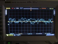
* Next 3 photos, yellow is the Victor oscillator input to the hall notch board, while blue is the Hall notch output adjusted for minimum level. As shown 200mV/div for the yellow and 500uV/div on the blue notch output.
* The last one 4693 is with the scope time base run way out (2.0 ns) to get a better look at the noise riding on the notch. I've had the scope freeze a snapshot here. Looks random.
Hovering over the photos will bring up the picture number, clicking on the lower right arrows will enlarge them.
Attachments
Last edited:
I've built a passive version of the Hall network. When I measured the output with a scope, I thought the notch depth was around 60dB, but it turned out it was the sensitivity of my scope that was limiting the measurement.
Later on I added a 60dB gain stage and measure the level with ARTA (the ADC of my sound card is much better than that of my scope, at audio frequency), and I realized the notch depth was almost 90dB.
Yours may vary, as it's active, and the component matching are very critical and will impact the depth a lot.
cwtim01 - hey very interesting! Thank you for letting me know. Can't argue with results, wow -90dB!!
The op-amps here may very well be having a (negative) effect and/or scope (lack of) sensitivity. I can bypass the input buffer easily enough, that would be an interesting first test. Then the positive feedback buffer could probably be replaced with a 1K + 1K voltage divider hanging off the output buffer op amp. The output OPA1641 should be able to drive 2K. 1K + 1K would keep the divider current >> than the current through the 10K frequency set pot. In fact I think I'll just build up another board that way rather than do surgery on this one. I should try using the QA401 too for better sensitivity than the scope. I'll try re-measuring this board with the QA401.
Thank you for letting me know. Can't argue with results, wow -90dB!! The op-amps here may very well be having a (negative) effect and/or scope (lack of) sensitivity. I can bypass the input buffer easily enough, that would be an interesting first test. Then the positive feedback buffer could probably be replaced with a 1K + 1K voltage divider hanging off the output buffer op amp. The output OPA1641 should be able to drive 2K. 1K + 1K would keep the divider current >> than the current through the 10K frequency set pot. In fact I think I'll just build up another board that way rather than do surgery on this one. I should try using the QA401 too for better sensitivity than the scope. I'll try re-measuring this board with the QA401.
Last edited:
Your scope will give you more info as an FFT when looking at this stuff. Its much easier to see in the frequency domain. You should see the fundamental and a few harmonics in the output.
You need the buffer for the positive feedback. It needs a very low impedance. I used LME49990's on the Shibasoku but any really good low noise opamp (AD797 or LT1115) would do the job.
Another trick if you can is to reduce the sample rate in the scope. Lower sample rates won't capture the HF stuff.
You need the buffer for the positive feedback. It needs a very low impedance. I used LME49990's on the Shibasoku but any really good low noise opamp (AD797 or LT1115) would do the job.
Another trick if you can is to reduce the sample rate in the scope. Lower sample rates won't capture the HF stuff.
Thanks for the suggestions! I'll give the FFT and lower sample rate a try.
Yeah I've just remembered that on the purely passive Hall notch, what cwtim01 is using, the wiper on the the Hall's frequency pot is actually grounded. So I can see you are right, that positive feedback path should likely also be very low Z looking back into it from the frequency pot wiper.
Yeah I've just remembered that on the purely passive Hall notch, what cwtim01 is using, the wiper on the the Hall's frequency pot is actually grounded. So I can see you are right, that positive feedback path should likely also be very low Z looking back into it from the frequency pot wiper.
Hall notch: -70dB with OPA1612 on a dual-chip board! Part 1
As the title says, I've measured a -70dB Hall notch this time using a OPA1612 dual op-amp on one of my dual-chip Hall notch filter boards! This is with the QA401 measuring the notch too, not the scope.
Details
The previous results above were with one of the "single op-amp output chip" boards I had made, that use singles for the output buffer and the feedback amp. That set of tests used FET-input OPA1641 chips. I wanted to try building up one of the dual output chip boards this time, with some slightly different parameters:
Photos and results
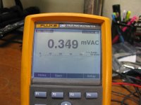
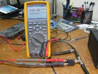
* 4749 shows the setup with the DMM, which is set to the mVac range and set to show measured frequency. This DMM is true rms, so all the AC readings here are rms. 0.34mVrms = 340uVrms, and 998Hz. I've known for awhile that Victor's 1KHz oscillator here runs a couple of Hz low.
* 4753 shows the input of the dual-chip board attached to the oscillator. Just shows there is a small 20uV loading of the Victor Oscillator, now at 320uVrms, and the oscillator has drifted up to 998.5Hz. This was taken 15 minutes or so after the other, so the drift is all thermal as the oscillator warms up.
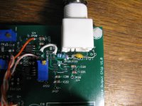
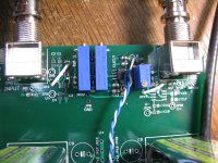
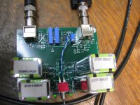
* 5755, 56, and 59 show the Hall notch dual-chip board. I located my other two lithium polymer "9V" batteries from the single chip tests above so both rails are now dual-battery. The rails are running at +16.4 and -16.2 here after I freshly charged all 4 batteries. It is actually normal for the batteries to be tilted at angles like this. Turns out the negative post on 9V cells is 0.5mm longer than the positive post. If you are laying them flat on a PCB the negative clip has to be 0.5 back from the other to make them be perpendicular. NwAvGuy's O2 didn't do this and the clips have to be bent a little to get the batteries straight. But here, with end mount, they just tilt at funny angles. If I ever do a board revision I'll probably flip the bottom two snaps so the batteries all tilt in the same direction on each side.
On the left, by the input jack, the white wire is the jumper across the un-populated IC1 input buffer. On the IC3 output gain chip on the right the white wire is a jumper across that un-populated chip. That just leaves the single dual-channel IC2 for the Hall notch output buffer and feedback factor buffer. Each power rail is bypassed with 4.7uf and 0.1uF, same as with the single-chip board previously, and a twisted pair is used to bring the power from the batteries.
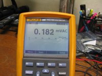
* 5760, 62, and 63 now show the notch output results on the DMM. 5760 is the initial output with nothing but the trimpots centered ohmically. Not bad! 22.5mVrms, down from the 320mVrms input. Rotating the frequency trimpot 5.5 turns counterclockwise resulted in the notch bottom of 349uVrms in 5762. Then rotating the notch depth trimpot 1/2 turn clockwise in 5763 dropped the notch bottom to its final resting place of 182 uVrms.
Doing the math, 0.182mV/320mV = 0.00057mV. Plugging into a dB calculator here
Decibels to Voltage Gain and Loss convert calculation conversion amplification amplifier electronics - sengpielaudio Sengpiel Berlin
comes up with -65dB! This is still with the DMM, of course. Below the tests with the QA401 come up with -70dB.
I've run out of photo slots, on to part 2 for the QA401 tests. The layout and schematic are attached here.
Clicking on the arrows in the lower right corner of the pictures will zoom them up, and hovering over the pictures will give their numbers.
As the title says, I've measured a -70dB Hall notch this time using a OPA1612 dual op-amp on one of my dual-chip Hall notch filter boards! This is with the QA401 measuring the notch too, not the scope.
Details
The previous results above were with one of the "single op-amp output chip" boards I had made, that use singles for the output buffer and the feedback amp. That set of tests used FET-input OPA1641 chips. I wanted to try building up one of the dual output chip boards this time, with some slightly different parameters:
- Don't use an input buffer, to eliminate some noise. The sims I've done show the Hall Notch circuit, with these values anyway, isn't critical about typical input impedance amounts (from the Victor Oscillator). Probably no need for the "near zero" impedance of the network looking back into the input buffer. The input buffer IC1 is then left off the board and jumpered across.
- For the dual-output-chip version here I wanted to use a bipolar OPA1612 vs the two single FET-input OPA1641's in the single-chip tests above. Again some more potential noise reduction with the bipolar op-amps. 1.1nV/sqrt(Hz) @ 1KHz vs. 5.1.
- I wanted to try using a DMM (fluke 289) to rough-in the notch rather than the scope this time, since I remembered the DMM is good to 100KHz and goes down to 1uVrms on the AC range.
- And then finally the good suggestion made above of using the QA401 to measure the notch depth for more accuracy.
Photos and results
* 4749 shows the setup with the DMM, which is set to the mVac range and set to show measured frequency. This DMM is true rms, so all the AC readings here are rms. 0.34mVrms = 340uVrms, and 998Hz. I've known for awhile that Victor's 1KHz oscillator here runs a couple of Hz low.
* 4753 shows the input of the dual-chip board attached to the oscillator. Just shows there is a small 20uV loading of the Victor Oscillator, now at 320uVrms, and the oscillator has drifted up to 998.5Hz. This was taken 15 minutes or so after the other, so the drift is all thermal as the oscillator warms up.
* 5755, 56, and 59 show the Hall notch dual-chip board. I located my other two lithium polymer "9V" batteries from the single chip tests above so both rails are now dual-battery. The rails are running at +16.4 and -16.2 here after I freshly charged all 4 batteries. It is actually normal for the batteries to be tilted at angles like this. Turns out the negative post on 9V cells is 0.5mm longer than the positive post. If you are laying them flat on a PCB the negative clip has to be 0.5 back from the other to make them be perpendicular. NwAvGuy's O2 didn't do this and the clips have to be bent a little to get the batteries straight. But here, with end mount, they just tilt at funny angles.
If I ever do a board revision I'll probably flip the bottom two snaps so the batteries all tilt in the same direction on each side.On the left, by the input jack, the white wire is the jumper across the un-populated IC1 input buffer. On the IC3 output gain chip on the right the white wire is a jumper across that un-populated chip. That just leaves the single dual-channel IC2 for the Hall notch output buffer and feedback factor buffer. Each power rail is bypassed with 4.7uf and 0.1uF, same as with the single-chip board previously, and a twisted pair is used to bring the power from the batteries.
* 5760, 62, and 63 now show the notch output results on the DMM. 5760 is the initial output with nothing but the trimpots centered ohmically. Not bad!
22.5mVrms, down from the 320mVrms input. Rotating the frequency trimpot 5.5 turns counterclockwise resulted in the notch bottom of 349uVrms in 5762. Then rotating the notch depth trimpot 1/2 turn clockwise in 5763 dropped the notch bottom to its final resting place of 182 uVrms.Doing the math, 0.182mV/320mV = 0.00057mV. Plugging into a dB calculator here
Decibels to Voltage Gain and Loss convert calculation conversion amplification amplifier electronics - sengpielaudio Sengpiel Berlin
comes up with -65dB! This is still with the DMM, of course. Below the tests with the QA401 come up with -70dB.
I've run out of photo slots, on to part 2 for the QA401 tests. The layout and schematic are attached here.
Clicking on the arrows in the lower right corner of the pictures will zoom them up, and hovering over the pictures will give their numbers.
Attachments
-
 IMG_4762.JPG503.8 KB · Views: 48
 -
 IMG_4763.JPG454.9 KB · Views: 42
 -
hall notch filter schematic.pdf31.3 KB · Views: 67
-
 Hall notch filter layout.jpg531.9 KB · Views: 43
 -
 IMG_4760.JPG669.5 KB · Views: 48
 -
 IMG_4759.JPG464.2 KB · Views: 43
 -
 IMG_4756.JPG556.5 KB · Views: 49
 -
 IMG_4755.JPG552.8 KB · Views: 49
 -
 IMG_4753.JPG687.8 KB · Views: 50
 -
 IMG_4749.JPG647.9 KB · Views: 59
Last edited:
Hall notch: -70dB with OPA1612 on a dual-chip board! Part 2
Continuing on from above...
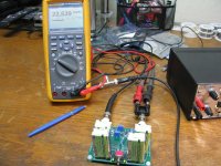
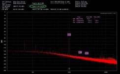
Photo 4764 shows the test setup now with the QA401 measuring the oscillator output on the left channel (yellow) and Hall notch filter output on the right channel (red).
The first QA401 plot in yellow for the Victor Oscillator output comes up with 320mVrms, up at the top circled in green! A wonderful double-check on the 319mVrms the DMM came up with. The measured frequency, M0 in purple on the screen, is now up to 999.75Hz as the Victor Oscillator continues to warm up, another gain of 1Hz.
Notice on the left axis, and the numbers above the green circle, the level is -9.89dBV, essentially -10dBV. This will make the notch depth easy to read in a minute.
The second QA401 plot in red is the notch output, 99.2uVrms in the green circle at the top. Also above that at the top is the -80dBV level. So just subtract from the above: -80dBV - (-10dBV) = -70dBV! Or doing the math, 0.0992mV/320mV = 0.00031, or -70.2dBV.
The big difference between the QA401 -70dB notch bottom and the DMM -65dB bottom is 100uV less in the notch measurement. I would tend to believe the QA401 number, just due to likely less internal noise at those small levels than the DMM, plus shielded BNC leads involved vs. just test leads for the DMM. Comparing the red notch output plot with the yellow input plot, it appears the Hall Notch board is adding 15dBV of noise below 1KHz. The board is sized to fit in a B2-080 metal case. That may be the next thing to try, with external power feed. Maybe the box will drop that noise figure a bit. I'm seeing a lot of (60Hz here) powerline harmonics in the output, but everything is battery powered. A portion of that noise must be external pickup.
All in all I'm quite pleased with the Hall notch filter at this point! -70dB does the job. Easy to tune, stable, fairly wide notch bottom, and this version uses just a single chip.
Happy holidays!
Continuing on from above...
Photo 4764 shows the test setup now with the QA401 measuring the oscillator output on the left channel (yellow) and Hall notch filter output on the right channel (red).
The first QA401 plot in yellow for the Victor Oscillator output comes up with 320mVrms, up at the top circled in green! A wonderful double-check on the 319mVrms the DMM came up with. The measured frequency, M0 in purple on the screen, is now up to 999.75Hz as the Victor Oscillator continues to warm up, another gain of 1Hz.
Notice on the left axis, and the numbers above the green circle, the level is -9.89dBV, essentially -10dBV. This will make the notch depth easy to read in a minute.
The second QA401 plot in red is the notch output, 99.2uVrms in the green circle at the top. Also above that at the top is the -80dBV level. So just subtract from the above: -80dBV - (-10dBV) = -70dBV! Or doing the math, 0.0992mV/320mV = 0.00031, or -70.2dBV.
The big difference between the QA401 -70dB notch bottom and the DMM -65dB bottom is 100uV less in the notch measurement. I would tend to believe the QA401 number, just due to likely less internal noise at those small levels than the DMM, plus shielded BNC leads involved vs. just test leads for the DMM. Comparing the red notch output plot with the yellow input plot, it appears the Hall Notch board is adding 15dBV of noise below 1KHz. The board is sized to fit in a B2-080 metal case. That may be the next thing to try, with external power feed. Maybe the box will drop that noise figure a bit. I'm seeing a lot of (60Hz here) powerline harmonics in the output, but everything is battery powered. A portion of that noise must be external pickup.
All in all I'm quite pleased with the Hall notch filter at this point! -70dB does the job. Easy to tune, stable, fairly wide notch bottom, and this version uses just a single chip.
Happy holidays!
Attachments
Last edited:
Hall notch board V2.0 experiments - linear trimpots - part 1
More fun with the Hall notch filter circuit.
I've just had a new round of V 2.0 test boards fabricated, a single op-amp and dual op-amp board similar to the previous set. Both have 15-turn 3/4" linear front-facing trimpots now for the frequency adjust and notch depth adjust. The goal here is to be able to finally get it boxed up in a metal B2-080 case to reduce noise pickup. I've left the feedback factor pot as the 25-turn 3/8" square since it doesn't do much.
In addition, on the single op-amp board, I've added pads around the feedback factor op-amp to convert it into an all-pass filter to introduce a degree or so of phase lead or lag. I want to test the EDN author's theory that phase shift in the op amps was reducing notch depth a bit.
Some other changes -
* A ground hole near the frequency trimpot wiper on both boards to allow them to be configured simply as passive Hall notch filters, with no op-amps.
* Pads for an output series resistor, followed by a capacitor to ground. Can be used for cable capacitance isolation and/or adding a low pass filter on the output, as per the great suggestion in the posts above.
* The battery snaps all go in the same direction now so the batteries line up. Looks better.
* I tracked down the part number for the metal version of the PC mount BNC connectors I've been using and have used those in the build-up.
* Silk screen circles around the power supply holes, vs just the test points. On the previous builds I kept getting those mixed up.
I've also gone through the EDN math again to come up with a set of values for a narrower range, 900Hz to 1.2KHz, vs. the article's original 750Hz to 1.5KHz. The simulation results were not good though, so in the build-up here I've continued to use the original 0.75 - 1.5K range. With the narrower range the notch bottom is much more narrow. Just 1Hz of drift is all it would take to pop 20dB out of the notch well on either side. With the original range the notch bottom is several Hz wide, which takes some Victor oscillator thermal drift into account. The phase shift of the filter also appears to not be as symmetrical with the narrower range. I've attached the workup for the narrower 0.9KHz - 1.2KHz range below, even though I'm not using it, in case anybody else wants to mess with it. There are a couple of notes in there too on what I've found the EDN author did.
The build-up here is for the dual op-amp board. I've attached schematics and layout for both boards.
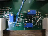
The first 5 photos show the test setup with a Victor oscillator and DMM. I'm using the DMM method to rough the notch in again since that worked so well last time. The pots were all ohmically centered before soldering. Once again the notch was already down from the 340mVac(rms) input to 20mVac(rms) just with centering. Then about 4 turns clockwise of the frequency trimpot from there to find the notch minimum. Then rotating the notch depth pot just about 1/4 turn counterclockwise came up with the final notch bottom of 200uVac(rms). The linear trimpot on the left (board oriented with the batteries at the PCB bottom) is the frequency pot. The one to the right of it is the notch depth (50K).
I bought several of each trimpot and went through them to find the closest match to 10K and 50K. Some of the 10K's were 950R total resistance (10% pot). The pots I used here measured 10.1K and 49.9K.
I have the input buffer stage and output gain stage both un-populated and jumpered across again. 10K input resistor, same as before.
Clicking on the arrows in the lower right corner of the pictures will zoom them up, and hovering over the pictures will give their numbers.
Out of photo posting slots, on to part 2 below...
More fun with the Hall notch filter circuit.
I've just had a new round of V 2.0 test boards fabricated, a single op-amp and dual op-amp board similar to the previous set. Both have 15-turn 3/4" linear front-facing trimpots now for the frequency adjust and notch depth adjust. The goal here is to be able to finally get it boxed up in a metal B2-080 case to reduce noise pickup. I've left the feedback factor pot as the 25-turn 3/8" square since it doesn't do much.
In addition, on the single op-amp board, I've added pads around the feedback factor op-amp to convert it into an all-pass filter to introduce a degree or so of phase lead or lag. I want to test the EDN author's theory that phase shift in the op amps was reducing notch depth a bit.
Some other changes -
* A ground hole near the frequency trimpot wiper on both boards to allow them to be configured simply as passive Hall notch filters, with no op-amps.
* Pads for an output series resistor, followed by a capacitor to ground. Can be used for cable capacitance isolation and/or adding a low pass filter on the output, as per the great suggestion in the posts above.
* The battery snaps all go in the same direction now so the batteries line up. Looks better.
* I tracked down the part number for the metal version of the PC mount BNC connectors I've been using and have used those in the build-up.
* Silk screen circles around the power supply holes, vs just the test points. On the previous builds I kept getting those mixed up.
I've also gone through the EDN math again to come up with a set of values for a narrower range, 900Hz to 1.2KHz, vs. the article's original 750Hz to 1.5KHz. The simulation results were not good though, so in the build-up here I've continued to use the original 0.75 - 1.5K range. With the narrower range the notch bottom is much more narrow. Just 1Hz of drift is all it would take to pop 20dB out of the notch well on either side. With the original range the notch bottom is several Hz wide, which takes some Victor oscillator thermal drift into account. The phase shift of the filter also appears to not be as symmetrical with the narrower range. I've attached the workup for the narrower 0.9KHz - 1.2KHz range below, even though I'm not using it, in case anybody else wants to mess with it. There are a couple of notes in there too on what I've found the EDN author did.
The build-up here is for the dual op-amp board. I've attached schematics and layout for both boards.
The first 5 photos show the test setup with a Victor oscillator and DMM. I'm using the DMM method to rough the notch in again since that worked so well last time. The pots were all ohmically centered before soldering. Once again the notch was already down from the 340mVac(rms) input to 20mVac(rms) just with centering. Then about 4 turns clockwise of the frequency trimpot from there to find the notch minimum. Then rotating the notch depth pot just about 1/4 turn counterclockwise came up with the final notch bottom of 200uVac(rms). The linear trimpot on the left (board oriented with the batteries at the PCB bottom) is the frequency pot. The one to the right of it is the notch depth (50K).
I bought several of each trimpot and went through them to find the closest match to 10K and 50K. Some of the 10K's were 950R total resistance (10% pot). The pots I used here measured 10.1K and 49.9K.
I have the input buffer stage and output gain stage both un-populated and jumpered across again. 10K input resistor, same as before.
Clicking on the arrows in the lower right corner of the pictures will zoom them up, and hovering over the pictures will give their numbers.
Out of photo posting slots, on to part 2 below...
Attachments
-
hall notch filter V2.0 single out schematic 15.pdf34.7 KB · Views: 66
-
 hall notch filter V2.0 single out layout 15.jpg578.9 KB · Views: 39
 -
hall notch filter V2.0 dual out schematic 19.pdf32.3 KB · Views: 80
-
 hall notch filter V2.0 dual out layout 19.jpg548.8 KB · Views: 53
 -
New hall notch range calculation 1.pdf45.6 KB · Views: 69
-
 IMG_4853.JPG644.6 KB · Views: 38
 -
 IMG_4850.JPG617.8 KB · Views: 46
 -
 IMG_4849.JPG665.5 KB · Views: 51
 -
 IMG_4848.JPG689.8 KB · Views: 52
 -
 IMG_4854.JPG557.5 KB · Views: 33
Last edited:
- Status
- This old topic is closed. If you want to reopen this topic, contact a moderator using the "Report Post" button.
- Home
- Design & Build
- Equipment & Tools
- Hall notch filter test boards -56dB